Delay locked loop in semiconductor memory device and its clock locking method

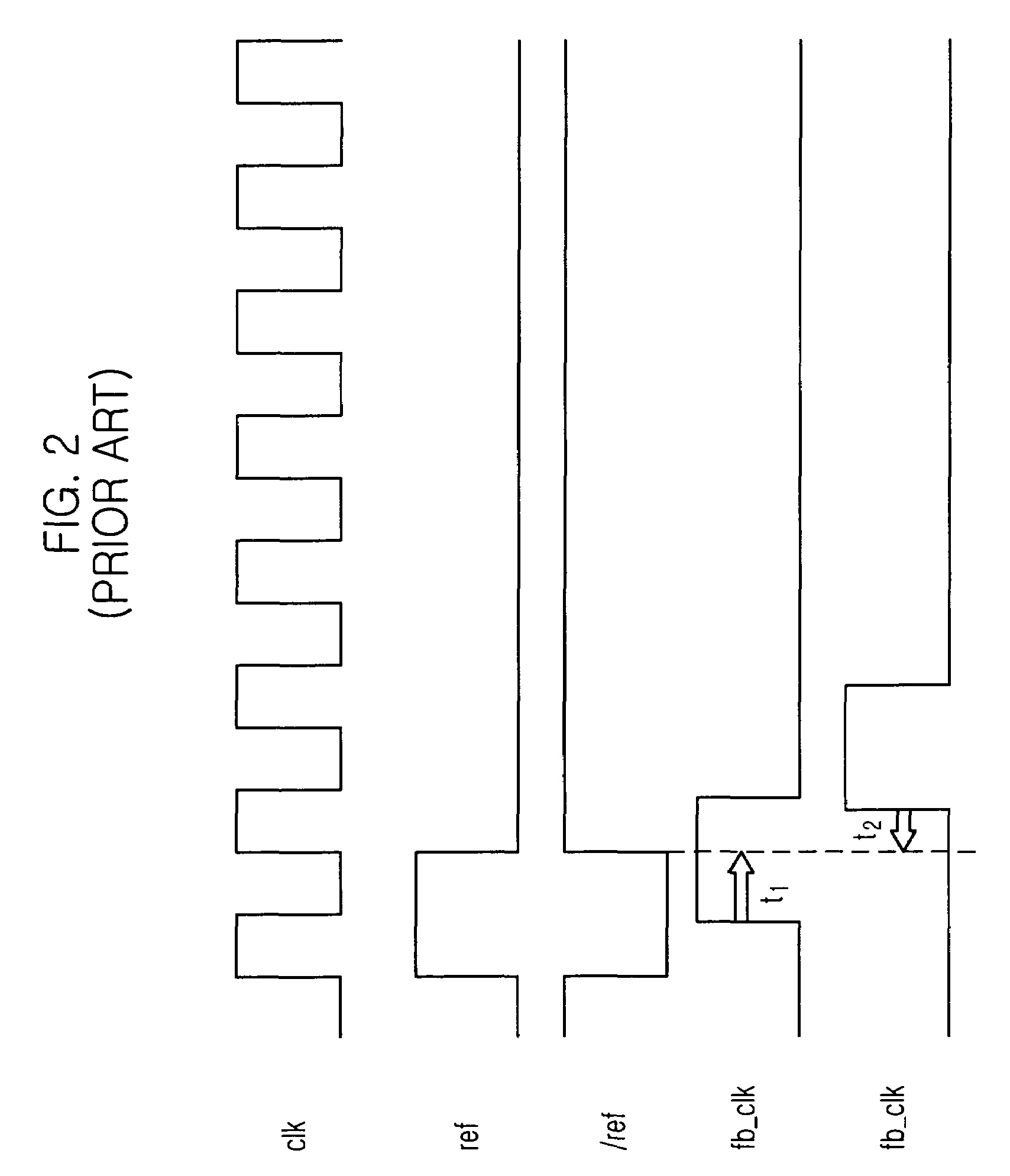
a semiconductor memory device and lock loop technology, applied in the direction of digital storage, pulse automatic control, generating/distributing signals, etc., can solve the problems of not generating a delay lock loop, the rise of the reference clock bar signal/ref and the feed-back clock signal fb/sub>clk cannot be synchronized, and the clock skew is generated between the external clock signal and the internal clock signal, etc. achieve stably operated operation, high operational frequency, and perform res

Active Publication Date: 2006-01-24
SK HYNIX INC
View PDF16 Cites 61 Cited by
  • Summary
  • Abstract
  • Description
  • Claims
  • Application Information

AI Technical Summary

Benefits of technology

[0024]It is, therefore, an object of the present invention to provide a DLL capable of preventing a clock skew, which is not compensable, from being generated, which is stably operated at a high operational frequency and performs a reset operation stably.

Problems solved by technology

When an external clock signal is inputted to a semiconductor memory device to be used as an internal clock signal, a clock skew is generated between the external clock signal and the internal clock signal because the external clock signal is delayed while it is inputted to the semiconductor memory device.
Therefore, rising edges of the reference clock bar signal / ref and the feed-backed clock signal fb—clk can not be synchronized.
As a result, because of a clock skew which is not compensable, the compensable the conventional DLL can not generate a delay locked clock signal.
However, since a pulse width of the reset signal is narrow, an operation for resetting the conventional DLL may not be performed stably.
However, if the feed-backed clock signal fb—clk may be generated due to the narrow pulse width of the reset signal, the phase comparator 103 may be operated abnormally.
However, the conventional DLL is not suitable for a semiconductor memory device operated at a high operational frequency because at the high operational frequency, the phase comparison operation should be more frequently performed.

Method used


Image

  • Delay locked loop in semiconductor memory device and its clock locking method
  • Delay locked loop in semiconductor memory device and its clock locking method
  • Delay locked loop in semiconductor memory device and its clock locking method

Examples


Embodiment Construction

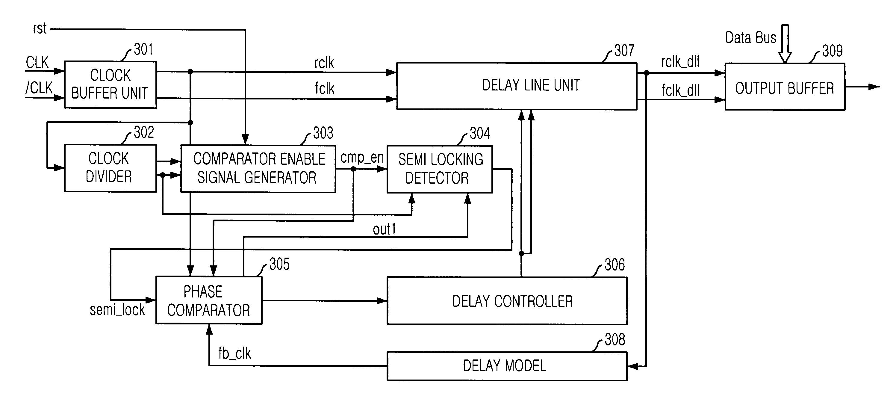
[0036]Hereinafter, a delay locked loop (DLL) for use in a semiconductor memory device in accordance with the present invention will be described in detail referring to the accompanying drawings.

[0037]FIG. 3 is block diagram showing a delay locked loop (DLL) in accordance with a preferred embodiment of the present invention.

[0038]As shown, the DLL includes a clock buffer unit 301, a clock divider 302, a comparator enable signal generator 303, a semi locking detector 304, a phase comparator 305, a delay controller 306, a delay line unit 307, a delay model 308 and an output buffer 309.

[0039]The clock buffer unit 301 receives an external clock signal CLK and an inverted signal of the external clock signal CLK, i.e., an external clock bar signal / CLK in order to generate a rising edge clock signal rclk and a falling edge clock signal fclk by buffering the external clock signal CLK and the external clock bar signal / CLK.

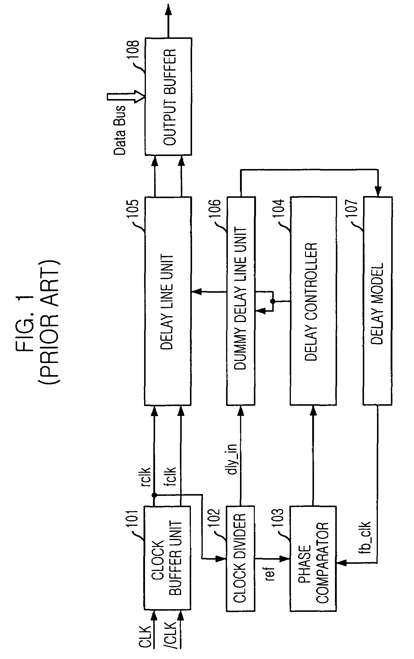
[0040]The clock divider 302 receives the rising edge clock signal rcl...


PUM


Abstract

A delay locked loop (DLL) for generating a delay locked clock signal, including: a comparator enable signal generator for generating a comparator enable signal in response to a reset signal and a plurality of clock divided signals; a semi locking detector for generating a semi locking detection signal in response to the comparator enable signal; a phase comparator enabled by the comparator enable signal for receiving a rising edge clock signal and a feed-backed clock signal in order to compare phases of the rising edge clock signal and the feed-backed clock signal and output the comparison result; and a DLL generator for generating the delay locked clock signal in response to the comparison result, wherein the comparator enable signal is generated by enlarging a pulse width of the reset signal by a predetermined amount.

Description

FIELD OF INVENTION[0001]The present invention relates to a delay locked loop (DLL); and, more particularly, to a DLL capable of being initialized stably in response to a reset signal.DESCRIPTION OF PRIOR ART[0002]Generally, a clock signal of a system or a circuit is used as a reference for synchronizing an execution timing and guaranteeing an error-free high speed operation.[0003]When an external clock signal is inputted to a semiconductor memory device to be used as an internal clock signal, a clock skew is generated between the external clock signal and the internal clock signal because the external clock signal is delayed while it is inputted to the semiconductor memory device. Therefore, various devices have been introduced to synchronize the internal clock signal with the external clock signal.[0004]For example, a phase locked loop (PLL) and a delay locked loop (DLL) have been developed in order to synchronize the internal clock signal with the external clock signal.[0005]Howev...

Claims


Application Information

Patent Timeline
Patent Type & Authority Patents(United States)
IPC IPC(8): H03L7/06G06F1/06G11C7/00G11C8/00G11C11/407G11C11/4076H03D13/00H03K5/13H03K5/26H03K21/00H03L7/08H03L7/081
CPCH03L7/0816H03L7/10H03L7/095H03L7/091G11C8/00
Inventor KIM, KYUNG-HOON
Owner SK HYNIX INC
Why Eureka
Try Eureka