Image distortion correcting device and image distortion correcting method

a technology of image distortion and correcting device, which is applied in the direction of instruments, television systems, pulse techniques, etc., can solve the problems of large current amount, difficult to correct the inner pincushion distortion, and significant image distortion, so as to improve the accuracy of image correction, the effect of not increasing the power consumption and correcting the image distortion

Inactive Publication Date: 2006-01-24
PANASONIC CORP
View PDF20 Cites 18 Cited by
  • Summary
  • Abstract
  • Description
  • Claims
  • Application Information

AI Technical Summary

Benefits of technology

[0008]An object of the present invention is to provide a low-cost image distortion correcting apparatus capable of correcting distortion in an image without increasing consumed power and an image distortion correcting method.

Problems solved by technology

Since the difference in deflection in the horizontal direction is larger than that in the vertical direction, however, the distortion in the image significantly appears.
However, the amount of the current is large.
Therefore, it is difficult to correct the inner pincushion distortion by adjusting the deflection current in the deflection circuit while restraining the consumed power.
When the inner pincushion distortion is corrected in the deflection circuit, the circuit configuration becomes complicated, thereby preventing the cost from being reduced.

Method used


Image

  • Image distortion correcting device and image distortion correcting method
  • Image distortion correcting device and image distortion correcting method
  • Image distortion correcting device and image distortion correcting method

Examples


first embodiment

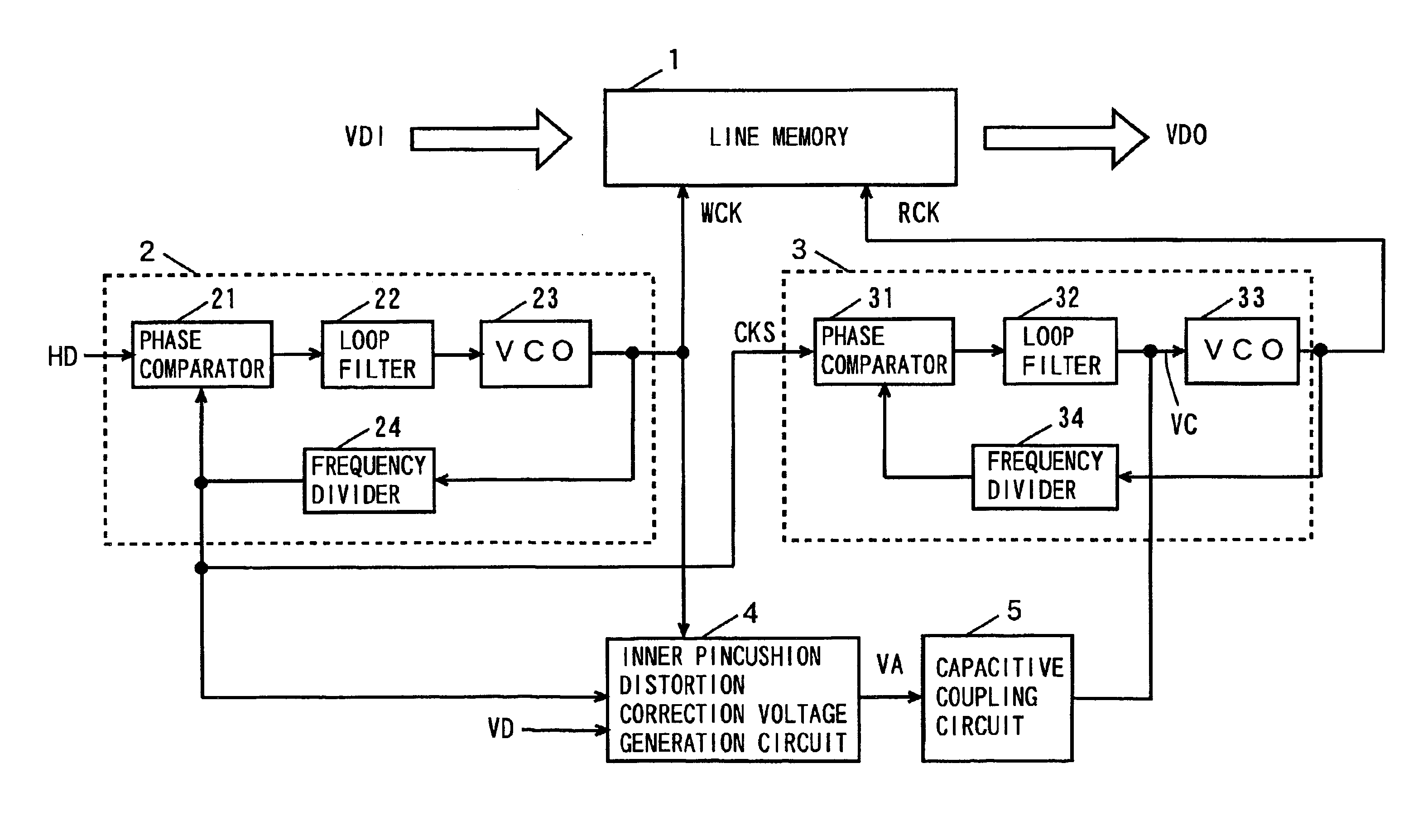
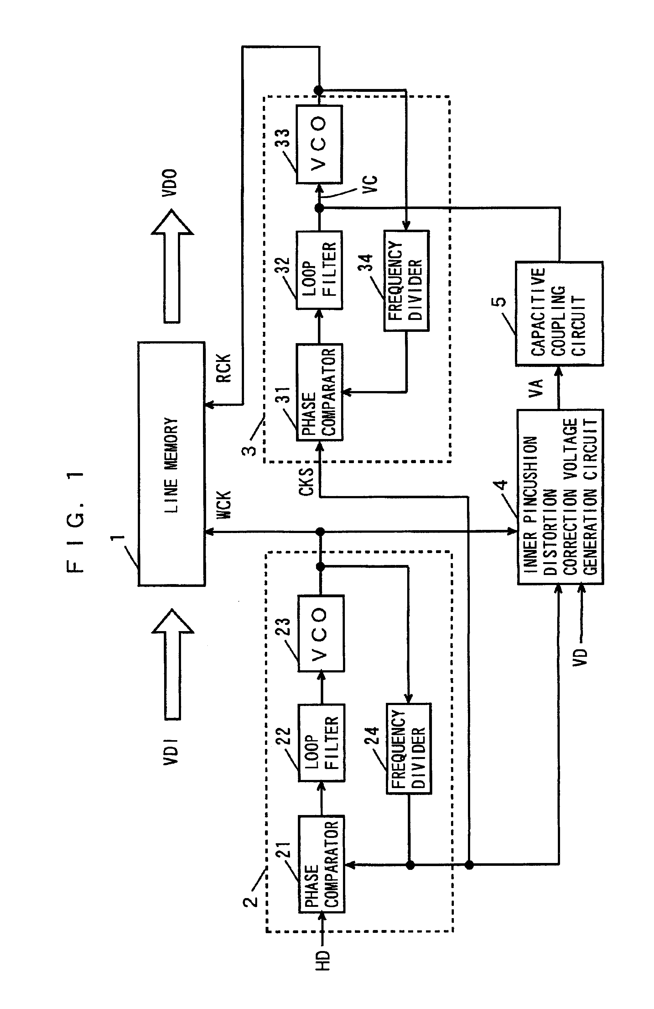
[0092]FIG. 1 is a block diagram showing the configuration of an image distortion correcting apparatus in the present invention.

[0093]The image distortion correcting apparatus shown in FIG. 1 comprises a line memory 1, a write PLL (Phase-Locked Loop) circuit 2, a readout PLL circuit 3, an inner pincushion distortion correction voltage generation circuit 4, and a capacitive coupling circuit 5. The write PLL circuit 2 comprises a phase comparator 21, a loop filter 22, a VCO (Voltage Controlled Oscillator) 23, and a frequency divider 24. Similarly, the readout PLL circuit 3 comprises a phase comparator 31, a loop filter 32, a VCO 33, and a frequency divider 34.

[0094]A horizontal synchronizing signal HD which is synchronized with a video signal VDI is fed to the phase comparator 21 in the write PLL circuit 2. The phase comparator 21 feeds a voltage corresponding to the phase difference between the horizontal synchronizing signal HD and an output signal of the frequency divider 24 to the ...

second embodiment

[0188]FIG. 19 is a block diagram showing an image distortion correcting apparatus in the present invention.

[0189]The image distortion correcting apparatus shown in FIG. 19 differs from the image distortion correcting apparatus shown in FIG. 1 in that an additional coupling circuit 6 is provided in place of the capacitive coupling circuit 5 shown in FIG. 1. An output voltage of a loop filter 32 is fed to the additional coupling circuit 6, and an output voltage of the additional coupling circuit 6 is fed to a VCO 33 as a control voltage VC. In the present embodiment, the additional coupling circuit 6 corresponds to a distortion correction waveform superimposing circuit.

[0190]FIG. 20 is a circuit diagram showing an example of the configuration of the readout PLL circuit 3 and the additional coupling circuit 6 shown in FIG. 19.

[0191]In FIG. 20, the additional coupling circuit 6 comprises an inversion adder 64, an inversion amplifier 65, and a non-inversion amplifier (a voltage follower)...


PUM


Abstract

A write PLL circuit generates a write clock signal for writing a video signal into a line memory. A readout PLL circuit generates a read clock signal for reading out the video signal stored in the line memory. An inner pincushion distortion correction voltage generation circuit modulates a correction waveform in the horizontal scanning period of time by a correction waveform in the vertical scanning period of time, to generate an inner pincushion distortion correction waveform, and adds a DC correction pulse to the inner pincushion distortion correction waveform and outputs the inner pincushion distortion correction waveform as an inner pincushion distortion correction voltage. A capacitive coupling circuit superimposes the inner pincushion distortion correction voltage on an output voltage of a loop filter of the readout PLL circuit, and feeds the inner pincushion distortion correction voltage to a VCO as a control voltage.

Description

TECHNICAL FIELD[0001]The present invention relates to an image distortion correcting apparatus and an image distortion correcting method for correcting distortion in an image displayed on a screen on the basis of a video signal.BACKGROUND ART[0002]In a CRT (Cathode-Ray Tube), an electron beam is deflected by a deflecting magnetic field and is irradiated onto its fluorescent surface, to display an image on a screen. The radius of the fluorescent surface of the CRT is larger than a radius from a deflecting center point of the electron beam to the fluorescent surface. Accordingly, the amount of movement of the electron beam in the periphery of the screen relative to the same amount of deflection is larger than the amount of movement of the electron beam at the center of the screen. As a result, when cross-hatched patterns which are inherently equally spaced are displayed on the screen, there occurs such a phenomenon that the spacing between the cross-hatched patterns is widened toward ...

Claims


Application Information

Patent Timeline
Patent Type & Authority Patents(United States)
IPC IPC(8): H04N3/26H04N3/23H04N5/14G09G1/00H04N3/233
CPCH04N3/2335H04N3/23
Inventor NAKATSUJI, MASANORITANAKA, MASANOBUUWABATA, HIDEYOOKUMURA, NAOJIYAMATE, KAZUNORI
Owner PANASONIC CORP
Why Eureka
Try Eureka