Display apparatus and method for fabricating the same

a technology of display apparatus and display device, which is applied in the manufacture of electric discharge tubes/lamps, cold cathode manufacturing, and the manufacture of electromechanical systems, etc., can solve the problems of significant degradation of display properties, voltage drop, and damage to devices, and achieve the effect of improving display properties and sufficient luminous intensity of organic el devices

Inactive Publication Date: 2006-01-31
JOLED INC
View PDF5 Cites 66 Cited by
  • Summary
  • Abstract
  • Description
  • Claims
  • Application Information

AI Technical Summary

Benefits of technology

[0016]It is therefore an object of the present invention to provide an active-matrix-type display apparatus ensuring sufficient luminous intensity of the organic EL devices and allowing improved display properties.
[0022]Since the rib having the conductive material serves as an auxiliary wiring for the second electrode, the pressure drop of the second electrode can successfully be suppressed and thus sufficient luminous intensity of the organic light emitting layer of the individual pixels can be retained even when the second electrode is made of a high-resistivity material. Moreover, the rib also serves as a spacer for a mask used for patterning the organic layer, so that there is no need to separately provide the spacer and the auxiliary wiring between every adjacent pixels. This allows space saving between every adjacent pixels and reserve of the pixel area.
[0030]According to the display apparatus according to the second aspect of the present invention, sufficient luminous intensity of the organic light emitting layer of all pixels on the display plane can be retained while achieving the space saving between every adjacent pixels to reserve sufficient pixel area by providing between every adjacent pixels the rib which serves as the spacers for the mask used for patterning the organic layer and also as the auxiliary electrode for the upper electrode covering the entire plane of the display plane. This results in improvement in the display properties of an active-matrix-type display apparatus.

Problems solved by technology

A problem will, however, arise in that there is a growing need for instantaneously applying a large current to the organic EL devices to ensure sufficient luminous intensity in the future situation in which the EL display apparatus will be operated at a higher duty responding to an increasing trend in the number of pixels, which is likely to damage the devices.
Such display apparatus having organic EL devices on the insulating film covering the TFTs on the substrate is, however, disadvantageous in that such TFTs are causative of narrowing the aperture of the organic EL devices when the display apparatus is designed as of transmission type in which light emitted from the organic layer is observed from the substrate side.
Indium tin oxide (ITO) and indium zinc oxide (IXO), known as materials for transparent conductive film, are however higher in resistivity than metals, so that the upper common electrode is likely to cause voltage drop due to internal voltage gradient occurs therein.
This may cause significant degradation of the display properties since the voltage applied to the individual organic EL devices on the display plane becomes non-uniform, and since the luminous intensity in the center portion of the display plane decreases.
While the transparent conductive film such as ITO or IXO can be formed by evaporation or sputtering, the former method is difficult to yield a film of good quality, and the obtained film tends to have high resistivity and low light transmissivity.
The sputtering is, however, higher in energy of particles to be deposited as compared with vapor deposition, so that the underlying surface on which the deposition proceeds is more likely to be damaged.
Since the basic structure of the organic EL device resembles to that of a light emitting diode made of inorganic semiconductor materials, such damages exerted on the underlying organic layer will be causative of leak current, which may further result in the production of non-emissive pixels called “dead pixels”.
Such metal film may, however, inevitably has a high sheet resistance as a result of the thinning and will also produce voltage gradient in the upper common electrode similarly to the case with the transparent conductive film, which will cause voltage drop and thus will significantly lower the display properties.
The thinning of the upper common electrode raises another problem in that the electrode cannot fully prevent the atmospheric moisture or oxygen from intruding into the organic layer, which will accelerate deterioration of the organic layer.

Method used


Image

  • Display apparatus and method for fabricating the same
  • Display apparatus and method for fabricating the same
  • Display apparatus and method for fabricating the same

Examples


Embodiment Construction

[0054]The present invention will be detailed referring to the attached drawings.

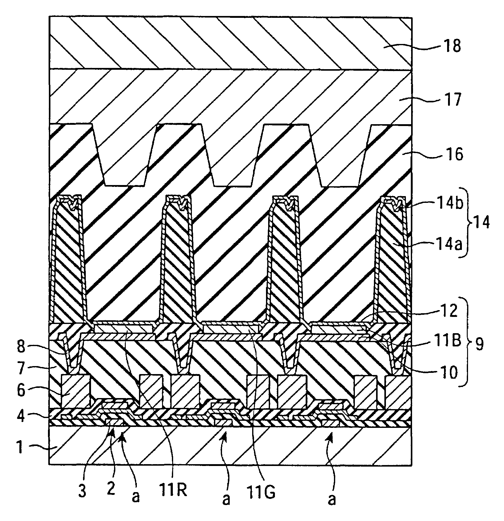
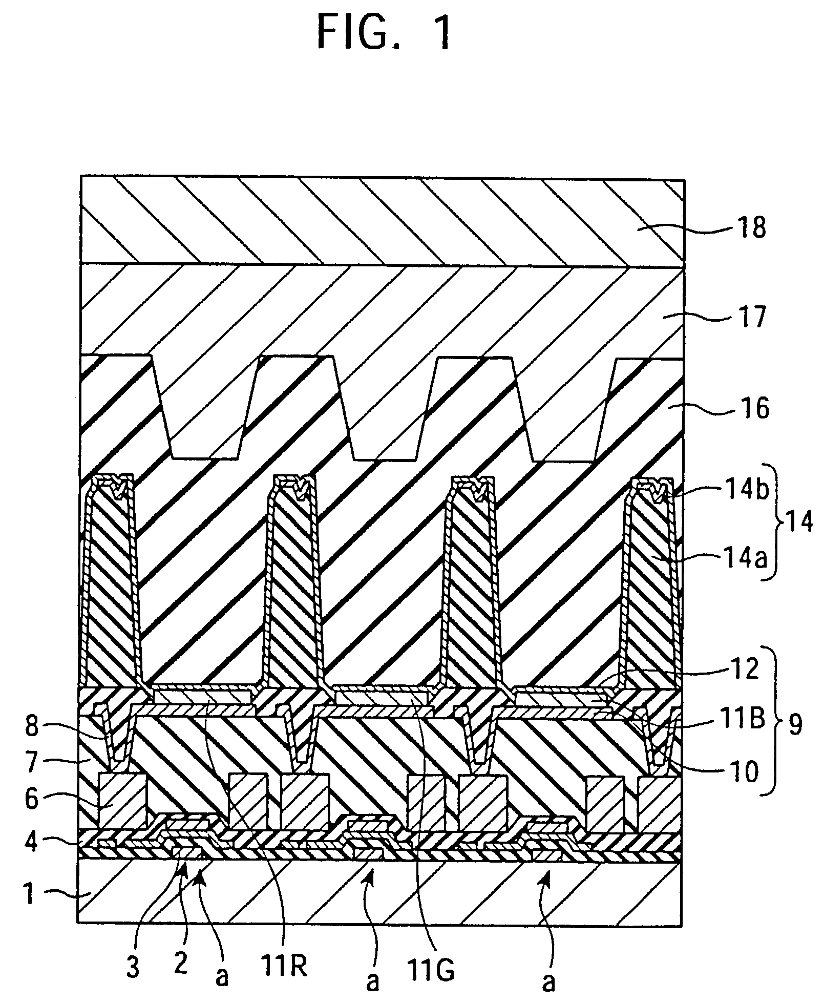
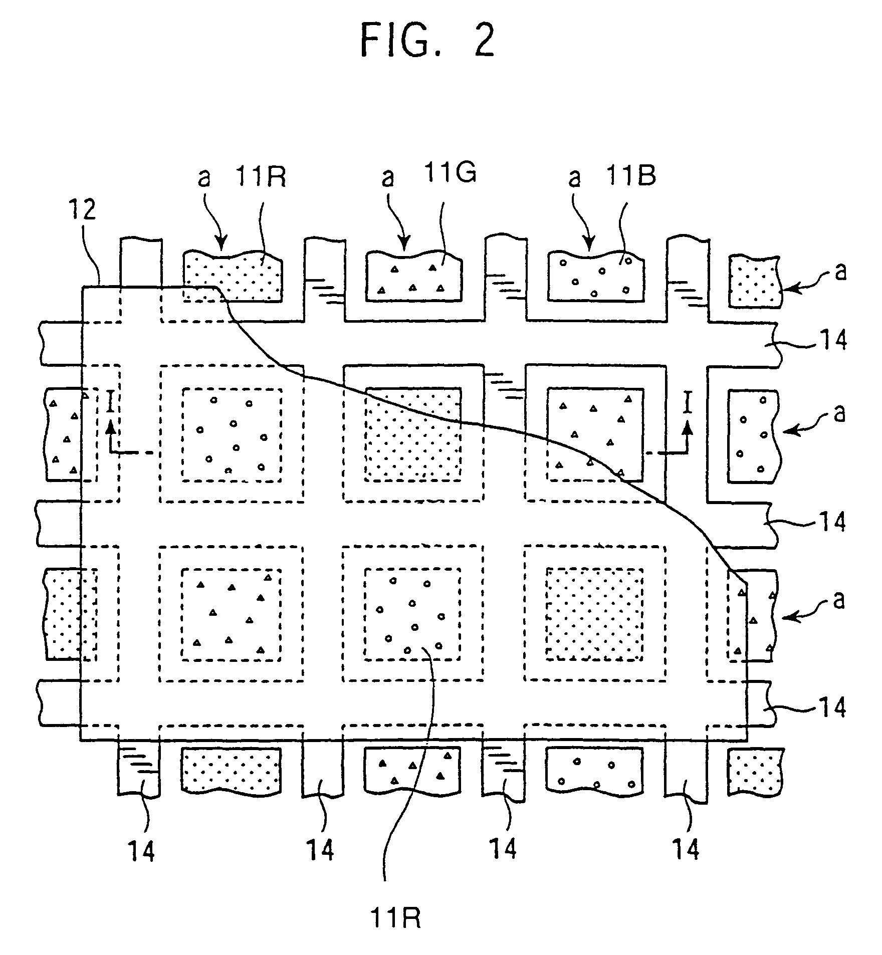
[0055]FIG. 1 is a schematic sectional view showing a display area of a display apparatus according to an example of the present invention. FIG. 2 is a schematic plan view showing the display area of the display apparatus shown in FIG. 1. FIG. 1 is a view in section along the line I—I in FIG. 2. Among various structural components which will be explained hereinafter in order from those closer to the lower layer side, FIG. 1 now shows only organic layers 11R, 11G, 11B, an upper common electrode 12 and ribs 14. The organic EL display apparatus shown in these figures is an active-matrix-type color display apparatus, the constitution of which will be explained with reference also to additional drawings of FIGS. 3A, 3B, 3C, 4, 5A, 5B. 5C, 6 and 7 following the fabrication procedures thereof.

[0056]First as shown in FIG. 3A, a thin-film transistor 2 is fabricated for every pixel “a” on a substrate 1. A gate elec...


PUM


Abstract

An active-matrix-type display apparatus ensuring sufficient luminous intensity of display devices within a display plane and allowing improved display properties is provided. Such display apparatus having of a plurality of pixels comprises a lower electrode formed on a substrate; organic layers formed on the lower electrode; and an upper common electrode formed on the organic layers; in which a plurality of the pixels are partitioned by a rib larger in the thickness than the organic layers and having at least a conductive material layer; and the conductive material layer is electrically connected to the upper common electrode.

Description

RELATED APPLICATION DATA[0001]The present application claims priority to Japanese Application No. P11-306245, filed Oct. 28, 1999, and is a divisional of U.S. application Ser. No. 09 / 698,989, filed Oct. 27, 2000 now U.S. Pat. No. 6,768,257, both of which are incorporated herein by reference to the extent permitted by law.BACKGROUND OF THE INVENTION[0002]1. Field of the Invention[0003]The present invention relates to a display apparatus which comprises organic electro-luminescence devises individually having an organic light emitting layer, and a method for fabricating such display apparatus.[0004]2. Description of the Related Art[0005]An organic electro-luminescence (abbreviated as EL hereinafter) device based on electro-luminescence of organic materials has an organic layer comprising an organic hole transport layer and an organic light emitting layer laminated between a lower electrode and an upper electrode, and is attracting a good deal of attention as a light emitting device ca...

Claims


Application Information

Patent Timeline
Patent Type & Authority Patents(United States)
IPC IPC(8): H01J9/00H01L21/77H01L21/84H01L27/32H01L51/52
CPCH01L27/1214H01L27/3246H01L51/5212H01L51/5228H01L51/5203H01L51/0011H01L2251/5315H10K59/122H10K71/166H10K50/814H10K50/824H10K2102/3026H10K59/805H10K50/805
Inventor YAMADA, JIROSASAOKA, TATSUYASEKIYA, MITSUNOBUSANO, NAOKICHIBA, YASUHIROHIRANO, TAKASHIIWASE, YUICHI
Owner JOLED INC
Why Eureka
Try Eureka