Gallium nitride based compound semiconductor light-emitting device

a compound semiconductor and light-emitting device technology, applied in semiconductor/solid-state device manufacturing, semiconductor devices, electrical equipment, etc., can solve the problems of ineffective stimulation of p-n structure, insufficient light-emitting efficiency of led, and insufficient conductivity of inventive tcl, etc., to achieve better light-emitting performance, improve light extraction, and improve light-transparency performance

Inactive Publication Date: 2006-01-31
SEMILEDS OPTOELECTRONICS CO LTD
View PDF3 Cites 13 Cited by
  • Summary
  • Abstract
  • Description
  • Claims
  • Application Information

AI Technical Summary

Benefits of technology

[0014]In an LED, the inventive TCL has better performance in light transparency as compared to Ni / Au owing to its large bandgap. Aid the poorer conductivity of the inventive TCL may be compensated with the Ni / Au material. Further, since the doped metal oxide TCL may be made bulky, the TCL may be treated to have more facets to increase light extraction, which is contrasted to the currently used Ni / Au TCL. Hence, the inventive doped metal oxide TCL and the corresponding adaptive layer, Ni / Au, may achieve a good combination as a TCL, superior to the current Ni / Au layer for the p-type electrode of the LED, i.e., the inventive combination may provide both good light transparency and ohmic contact characteristics.

Problems solved by technology

However, in marching into a brand new era replacing the current lighting facilities with LEDs, the luminous efficiency of an LED is still a significant issue, which has been challenging those skilled in the art for many years.
However, the electrical force lines resulted from between the p-type electrode and an n-type electrode may not uniformly distribute in the p-n structure in the device.
Hence, the electrical charges provided by the applied electrical bias may not efficiently stimulate the p-n structure, which is necessary for light generation.
Further, the p-type electrode is inhered with poor mobility as compared to that of the n-type electrode and thus the stimulation efficiency of the electric bias on the device may not be satisfactory.
However, Ni / Au is not a material with satisfactory light transparency and should thus be made considerably thin, about 0.005–0.2 μm.
Therefore, Ni / Au material may not be the most appropriate choice as a TCL for an LED in light transparency and extraction efficiency's view owing to the thickness issue.
Further, since such GaN based light emitting device with Ni / Au as the TCL may not be formed with more facets by use of surface treatment under the limitation of 0.005–0.2 μm of thickness of the Ni / Au layer, the light extraction efficiency stands little possibility to be promoted in terms of the Ni / Au layer.

Method used


Image

  • Gallium nitride based compound semiconductor light-emitting device
  • Gallium nitride based compound semiconductor light-emitting device
  • Gallium nitride based compound semiconductor light-emitting device

Examples


second embodiment

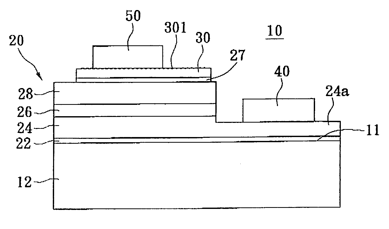
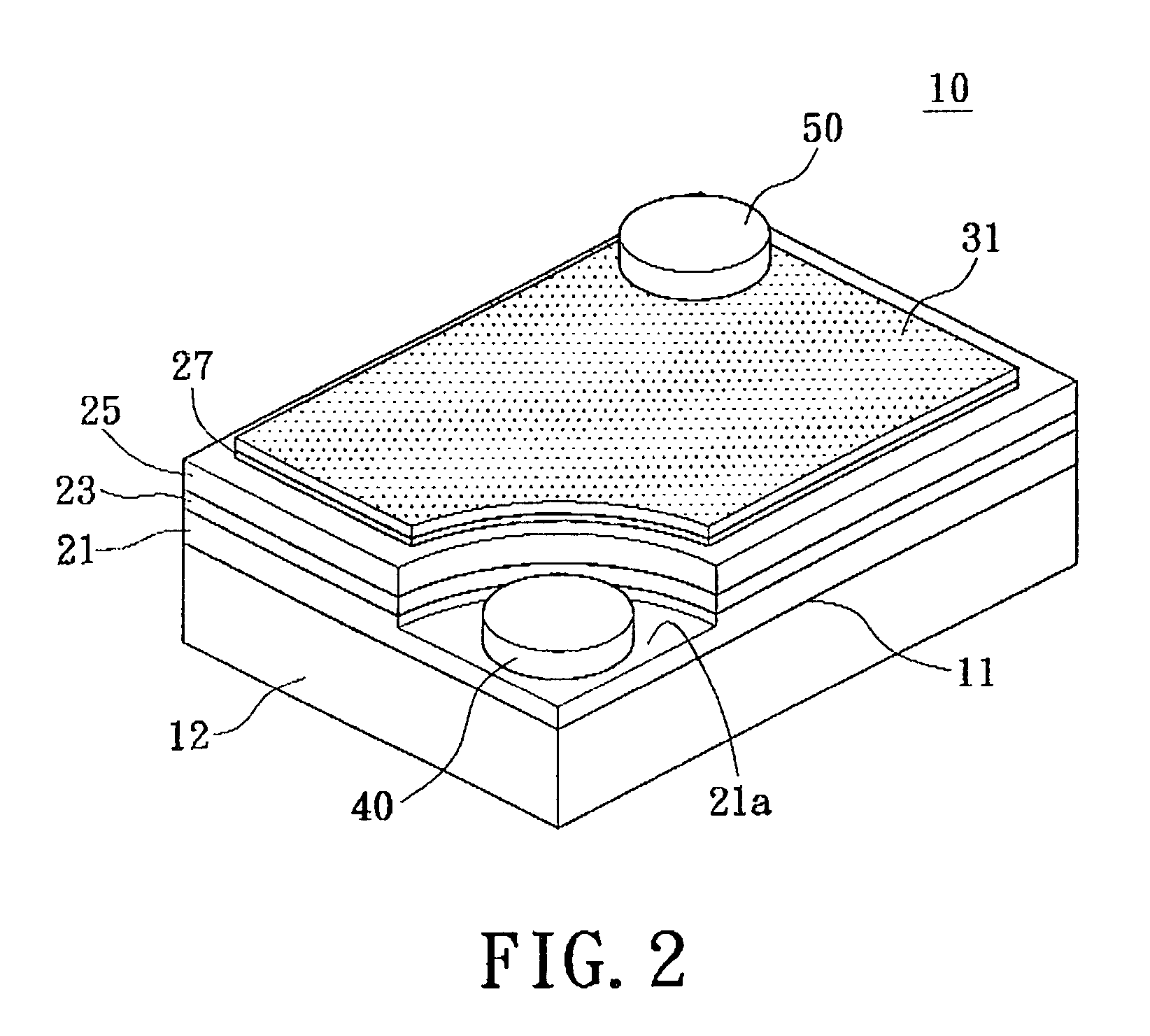
[0046]Referring to FIGS. 9 and 10, which illustrate the present invention. In the embodiment, transparent doped InxZn1−xO is used as the light extraction layer or window layer 32, wherein 0≦X≦1. The steps used in this embodiment are generally similar to those in the preferred embodiment except for the steps, Steps 5a and 6a, which are different from Steps 5 and 6 of the preferred embodiment. In this embodiment, Step 5a: forming an doped InxZn1−xO layer 32 over the Ni / Au layer 27. Similarly, the layer 27 serves as an ohmic contact layer and the layer 32 is preferably thicker than 1 μm. Step 6a: subjecting the doped InxZn1−xO layer 32 to a surface treatment. When the thickness of the layer 32 is larger than 1 μm, the layer 32 may be formed through a surface treatment as a roughened surface 321 or particularly textured surface.

third embodiment

[0047]Referring to FIGS. 11 and 12, which illustrate the present invention. In the embodiment, transparent doped SnxZn1−xO is used as the light extraction layer or window layer 33, wherein 0≦X≦1. The steps used in this embodiment are generally similar to those in the preferred embodiment except for the steps, Steps 5b and 6b, which are different from Steps 5 and 6 of the preferred embodiment. In this embodiment, Step 5b: forming a doped SnxZ1−xO layer 33 over the Ni / Au layer 27. Similarly, the layer 27 serves as an ohmic contact layer and the layer 33 is preferably thicker than 1 μm. Step 6b: subjecting the doped SnxZn1−xO layer 33 to a surface treatment. When the thickness of the layer 33 is larger than 1 μm, the layer 33 may be formed though a surface treatment as a roughened surface 331 or particularly textured surface.

fourth embodiment

[0048]Referring to FIGS. 13 and 14, which illustrate the present invention. In the embodiment, a transparent doped InxSnyZn1−yO layer is used as the light extraction layer or window layer 34, wherein 0≦X≦1, 0≦Y≦1 and 0≦X+Y≦1. The steps used in this embodiment are generally similar to those in the preferred embodiment except for the steps, Steps 5c and 6c, which are different from Steps 5 and 6 of the preferred embodiment. In this embodiment, Step 5c: forming a doped InxSnyZn1−yO layer 34 over the Ni / Au layer 27. Similarly, the layer 27 serves as an ohmic contact layer and the layer 34 is preferably thicker than 1 μm. Step 6c: subjecting the doped InxSnyZn1−yO layer 34 to a surface treatment. If the thickness of the layer 34 is made larger than 1 μm, the layer 34 may be formed through a surface treatment as a roughened surface 341 or particularly textured surface.

[0049]The dopants used in the doped metal oxide layer may at least be Al . Once the activation energy of the holes in this...


PUM


Abstract

Disclosed are a GaN based compound semiconductor light emitting diode (LED) and a manufacturing method therefor. In the LED, a combination of a light extraction layer and an adaptive layer is formed over a multi-layer epitaxial structure,wherein the light extraction layer is a light transmissible impurity doped metal oxide and the adaptive layer is a Ni/Au layer used to enhance ohmic contact between the light extraction layer and the multi-layer epitaxial structure.

Description

BACKGROUND OF THE INVENTION[0001]1. Field of the Invention[0002]The present invention relates to a GaN based compound semiconductor light-emitting device (LED) and a manufacturing method therefor, and particularly to a GaN based compound semiconductor light-emitting device (LED) with better light transparency and a manufacturing method therefor.[0003]2. Description og Related Art[0004]A light-emitting device (LFES) has been generally known as a device with ability to light generating, which has been widely used in digital watches, calculators, communications and other areas, such as mobile phone and some appliances. Recently, the efforts and attempts have shifted to use LEDs in more ordinary human living, such as large panels, traffic lights and lighting facilities. However, in marching into a brand new era replacing the current lighting facilities with LEDs, the luminous efficiency of an LED is still a significant issue, which has been challenging those skilled in the art for many ...

Claims


Application Information

Patent Timeline
Patent Type & Authority Patents(United States)
IPC IPC(8): H01L27/15H01L33/22H01L33/32H01L33/42
CPCH01L33/22H01L33/42H01L33/32
Inventor HON, SCHANG-JINGHUANG, JENN-BINYIH, NAI-GUANN
Owner SEMILEDS OPTOELECTRONICS CO LTD
Why Eureka
Try Eureka