Memory cell structure having nitride layer with reduced charge loss and method for fabricating same

a memory cell and nitride layer technology, applied in the direction of semiconductor devices, semiconductor/solid-state device details, electrical apparatus, etc., can solve the problems of unpredictable memory device behavior, affecting the performance of memory devices, so as to reduce the threshold voltage shift, reduce the charge loss and the method of fabricating

Inactive Publication Date: 2006-01-31
MONTEREY RES LLC
View PDF4 Cites 2 Cited by
  • Summary
  • Abstract
  • Description
  • Claims
  • Application Information

AI Technical Summary

Benefits of technology

[0006]The present invention is directed to a memory cell structure having nitride layer with reduced charge loss and method for fabricating same. The present invention addresses and resolves the need in the art for a memory cell structure which results in reduced threshold voltage shifts, reduced programmed data loss, reduced programming capability loss, and reduced device degradation.
[0007]According to one exemplary embodiment, the memory cell structure comprises a semiconductor substrate, a first silicon oxide layer situated over the semiconductor substrate, a charge storing layer situated over the first silicon oxide layer, a second silicon oxide layer situated over the charge storing layer, and a gate layer situated over the second silicon oxide layer. In the exemplary embodiment, the charge storing layer comprises silicon nitride having reduced hydrogen content, e.g., in the range of about 0 to 0.5 atomic percent. This reduced hydrogen content corresponds to a reduced hydrogen radical content which may be freed in the charge storing layer due to subsequent programming operations. As a result, the reduced hydrogen content in the charge storing layer reduces the charge loss in the charge storing layer. The reduction in charge loss in the charge storing layer has the benefit of reducing threshold voltage shifts, programming data loss, and programming capability loss in the memory device, thereby improving memory device performance. Reduced hydrogen content further corresponds to reduced hydrogen migration into adjacent layers.
[0008]The first silicon oxide layer, the charge storing layer, the second silicon oxide layer, and the gate layer form a gate stack having sidewalls. According to one exemplary embodiment, the memory cell structure further comprises spacers adjacent to the sidewalls of the gate stack. In this particular embodiment, each of the spacers comprises silicon nitride having reduced hydrogen content. As a benefit, the reduced hydrogen content in the spacers reduces the charge loss in the charge storing layer and the hydrogen migration into adjacent layers, thereby further improving memory device performance.

Problems solved by technology

Conventional techniques for forming the nitride layer of the ONO stack produce a number of negative effects, which detrimentally affect the performance of the memory device.
The sizable content of hydrogen in the nitride layer becomes detrimental, for example, when energetic electrons are injected into the nitride layer during subsequent programming cycles.
The presence of hydrogen radicals in the nitride layer produces a charge loss in the nitride layer, resulting in such negative effects as a shift in the threshold voltage of the memory cell, which results in unpredictable memory device behavior.
Furthermore, the charge loss in the nitride layer may further result in the loss of programming data and / or programming capability in the memory cell.
The hydrogen radicals may also migrate into the adjacent oxide layers, such as the top and bottom layers of the ONO stack and further degrade device properties.
These negative effects result in poor performance of the memory device.

Method used


Image

  • Memory cell structure having nitride layer with reduced charge loss and method for fabricating same
  • Memory cell structure having nitride layer with reduced charge loss and method for fabricating same
  • Memory cell structure having nitride layer with reduced charge loss and method for fabricating same

Examples


Embodiment Construction

[0014]The present invention is directed to a memory cell structure having nitride layer with reduced charge loss and method for fabricating same. The following description contains specific information pertaining to the implementation of the present invention. One skilled in the art will recognize that the present invention may be implemented in a manner different from that specifically discussed in the present application. Moreover, some of the specific details of the invention are not discussed in order not to obscure the invention.

[0015]The drawings in the present application and their accompanying detailed description are directed to merely exemplary embodiments of the invention. To maintain brevity, other embodiments of the present invention are not specifically described in the present application and are not specifically illustrated by the present drawings.

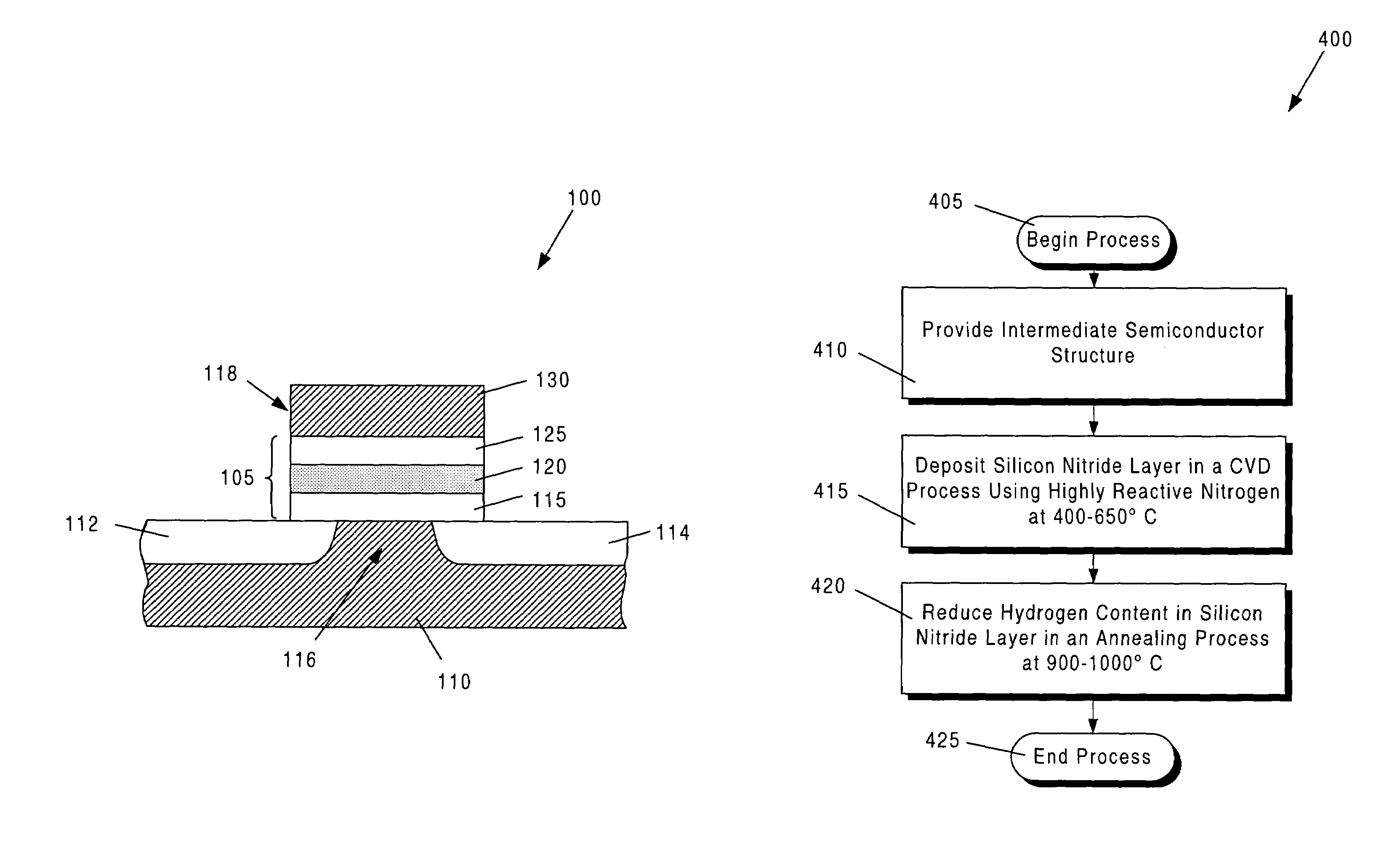
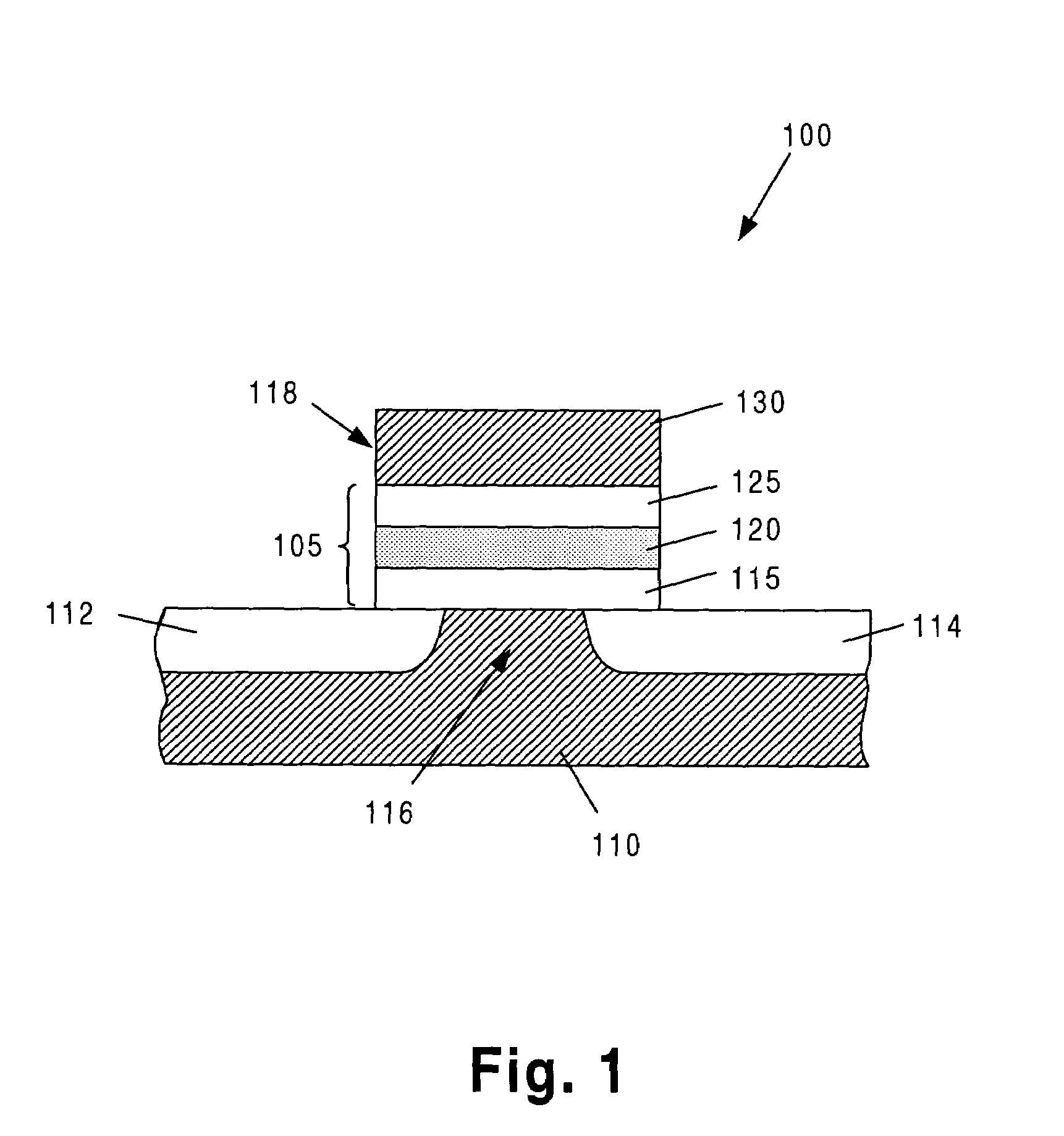
[0016]FIG. 1 depicts exemplary memory cell structure 100 according to one embodiment of the present invention. As describ...


PUM


Abstract

According to one embodiment, a memory cell structure comprises a semiconductor substrate, a first silicon oxide layer situated over the semiconductor substrate, a charge storing layer situated over the first silicon oxide layer, a second silicon oxide layer situated over the charge storing layer, and a gate layer situated over the second silicon oxide layer. In the exemplary embodiment, the charge storing layer comprises silicon nitride having reduced hydrogen content, e.g., in the range of about 0 to 0.5 atomic percent. As a result, the reduced hydrogen content reduces the charge loss in the charge storing layer. The reduced charge loss in the charge storing layer has the benefit of reducing threshold voltage shifts, programming data loss, and programming capability loss in the memory device, thereby improving memory device performance.

Description

TECHNICAL FIELD[0001]The present invention relates generally to the field of semiconductor devices. More particularly, the present invention relates to semiconductor memory devices.BACKGROUND ART[0002]Memory devices are known in the art for storing data in a wide variety of electronic devices and applications. More recently, SONOS (Silicon Oxide Nitride Oxide Silicon) type memory devices have been introduced. SONOS type flash memory cells comprise a gate stack having a gate layer situated over an ONO (Oxide Nitride Oxide) stack. The gate stack is situated over a semiconductor substrate where a channel region is defined between first and second terminals regions in the semiconductor substrate, thereby forming a transistor.[0003]The ONO stack comprises a non-conductive dielectric layer, typically a silicon nitride layer (“nitride layer”), positioned between two silicon oxide layers. The nitride layer functions as an electric charge storing medium. Moreover, the nitride layer is capabl...

Claims


Application Information

Patent Timeline
Patent Type & Authority Patents(United States)
IPC IPC(8): H01L23/58H01L21/302H01L21/28H01L21/336H01L21/8246H01L21/8247H01L27/115H01L29/51H01L29/788H01L29/792
CPCH01L21/28176H01L21/28202H01L21/28282H01L29/792H01L29/518H01L29/66833H01L29/513H01L29/40117H01L21/28167H01L29/51H01L29/511
Inventor KLUTH, GEORGE J.CLARK-PHELPS, ROBERT B.JEON, JOONG S.ZHONG, HUICAIHALLIYAL, ARVINDRAMSBEY, MARK T.OGLE, JR., ROBERT B.CHANG, KUO T.LI, WENMEI
Owner MONTEREY RES LLC
Why Eureka
Try Eureka