Barrier for interconnect and method

a technology of interconnection and barrier, which is applied in the field of barriers for interconnections, can solve the problems of increasing the number of current densities required for next generation technologies, reducing the dimensions of devices, and increasing clock speeds, and reducing the limits of conventional interconnect technology. , to achieve the effect of extending the reliability of current cmos designs, enhancing protection against voiding and delamination, and increasing current densities

Inactive Publication Date: 2006-01-31
INT BUSINESS MASCH CORP
View PDF9 Cites 3 Cited by
  • Summary
  • Abstract
  • Description
  • Claims
  • Application Information

AI Technical Summary

Benefits of technology

[0006]The invention includes a method of creating a multi-layered barrier for use in an interconnect, a barrier for an interconnect, and an interconnect including the barrier. The method includes creating the multi-layered barrier in a recess of a device terminal by use of a single electro-plating chemistry to enhance protection against voiding and de-lamination due to the diffusion of copper from the device terminal to the solder joint, whether by self-diffusion or electro-migration. The barrier includes at least a first layer of nickel-rich material and a second layer of copper-rich material. The barrier enables use of higher current densities for advanced complementary metal-oxide semiconductors (CMOS) designs, and extends the reliability of current CMOS designs regardless of solder selection. Moreover, this technology is easily adapted to current methods of fabricating electroplated interconnects such as controlled collapse chip connectors (C4) or ball grid array connectors.

Problems solved by technology

Reduction of device dimensions and increased clock speeds strain the limits of conventional interconnect technology.
For example, higher current densities required for next generation technologies present a number of problems.
One problem is that increased current densities increase the likelihood of voiding and de-lamination in under bump metallurgy (BLM) structure of a device terminal.
However, the presence of nickel alone was found insufficient to prevent voiding and de-lamination of titanium-tungsten (TiW), chromium-copper (CrCu) or copper (Cu) of the BLM structure, especially when the device was joined to a substrate using a nickel-gold (Ni—Au) pad.
Unfortunately, this requires two plating baths to deposit both nickel and copper layers.
While the use of a single bath is advantageous, that approach, designed on generating pure nickel and pure copper layers, does not take into consideration difficulties of plating the structure in the recess of a photoresist patterned wafer.

Method used


Image

  • Barrier for interconnect and method
  • Barrier for interconnect and method
  • Barrier for interconnect and method

Examples


Embodiment Construction

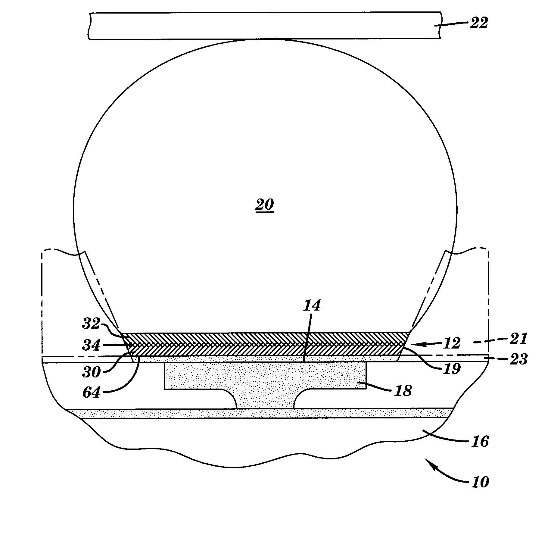
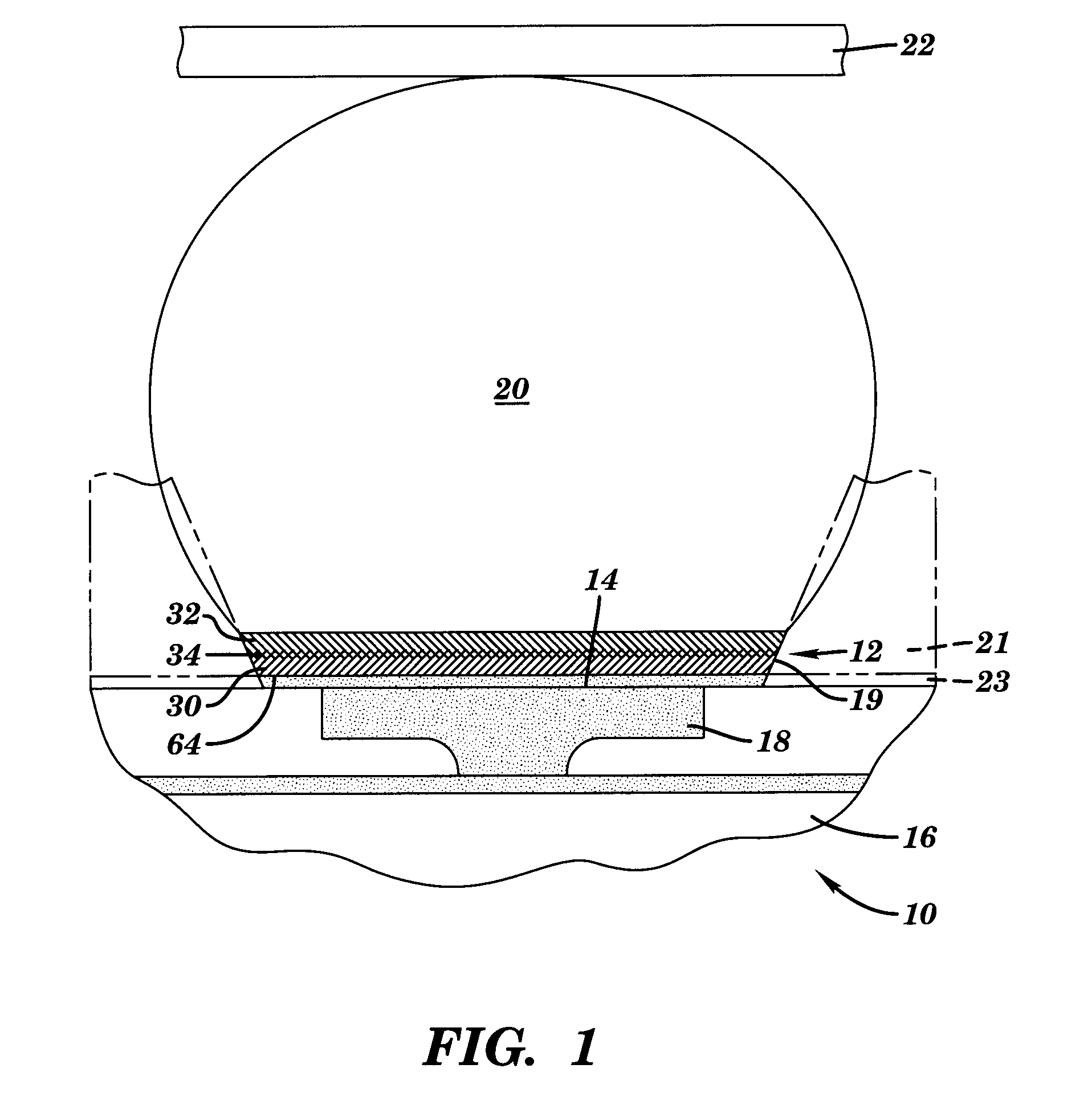
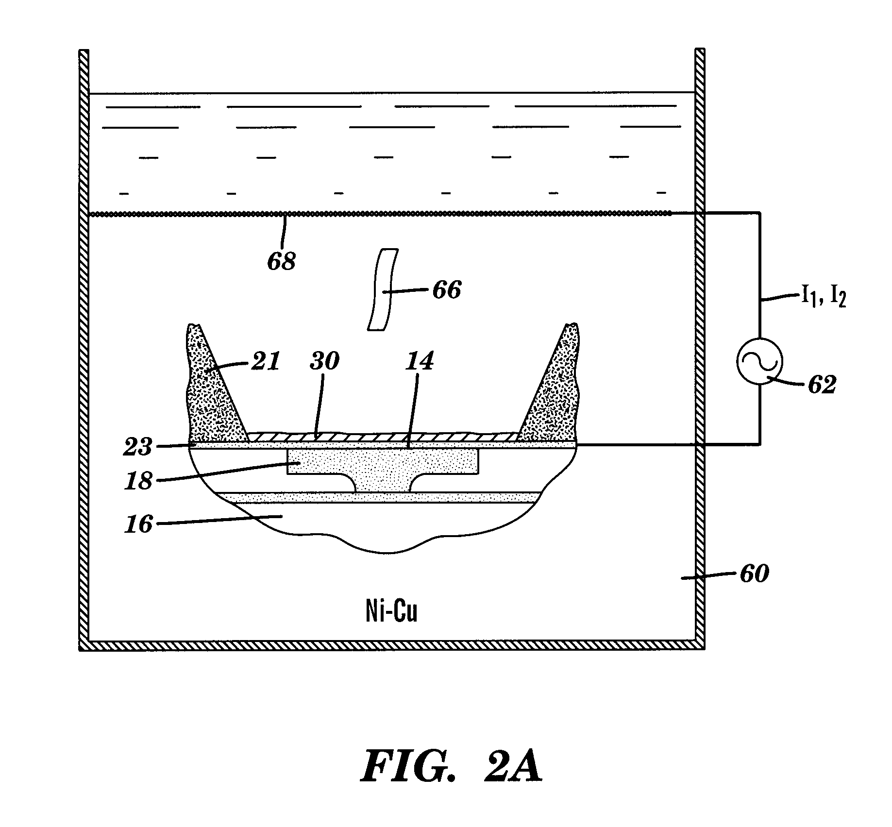
[0014]With reference to the accompanying drawings, FIG. 1 illustrates an interconnect 10 having a barrier 12 for preventing voiding and de-lamination in a device terminal 14 including an under bump metallurgy (UBM) seed layer 23 due to thermal diffusion and electro-migration of copper. In accordance with the invention, interconnect 10 includes device terminal 14 electrically connected to a semiconductor device 16, i.e., a via or contact 18 of semiconductor device 16. Device terminal 14 is formed in a patterned recess or hole 19 of a photoresist mask 21 (shown in phantom in FIG. 1). It should be recognized, however, that photoresist is an illustrative material, i.e., recess 19 may be provided in other material. All of photoresist mask 21 and UBM seed layer 23 outside of barrier 12 do not constitute part of the final device, but are shown in FIG. 1 in phantom for brevity. In one embodiment, recess 19 preferably has an aspect ratio, i.e., depth to width between 0.5 to 2.

[0015]In one em...


PUM


Abstract

A method of creating a multi-layered barrier for use in an interconnect, a barrier for an interconnect, and an interconnect including the barrier are disclosed. The method includes creating the multi-layered barrier in a recess of the device terminal by use of a single electroplating chemistry to enhance protection against voiding and de-lamination due to the diffusion of copper, whether by self-diffusion or electro-migration. The barrier includes at least a first layer of nickel-rich material and a second layer of copper-rich material. The barrier enables use of higher current densities for advanced complementary metal-oxide semiconductors (CMOS) designs, and extends the reliability of current CMOS designs regardless of solder selection. Moreover, this technology is easily adapted to current methods of fabricating electroplated interconnects such as C4s.

Description

BACKGROUND OF INVENTION[0001]The present invention relates generally to interconnects, and more particularly to a barrier for an interconnect and method of forming same.[0002]Reduction of device dimensions and increased clock speeds strain the limits of conventional interconnect technology. For example, higher current densities required for next generation technologies present a number of problems. One problem is that increased current densities increase the likelihood of voiding and de-lamination in under bump metallurgy (BLM) structure of a device terminal. In particular, the increased current densities increase thermal diffusion and electro-migration of copper from the BLM structure to the solder joint. This failure mode is especially possible for systems employing solders with high concentrations of tin (Sn) such as the leading lead-free solders or the eutectic lead-tin (PbSn) solders.[0003]In one approach, a nickel-only barrier was attempted. However, the presence of nickel alo...

Claims


Application Information

Patent Timeline
Patent Type & Authority Patents(United States)
IPC IPC(8): H01L23/48H01L23/485H01L23/52H01L21/60H01L21/288H01L21/4763
CPCH01L21/2885H01L24/05H01L24/13H01L24/11H01L2924/0001H01L2224/13111H01L2924/0105H01L2924/01033H01L2924/01024H01L2924/04953H01L2924/014H01L2924/01322H01L2924/01082H01L2224/0401H01L2224/05155H01L2224/05647H01L2224/13099H01L2924/01013H01L2924/01022H01L2924/01027H01L2924/01029H01L2924/01073H01L2924/01074H01L2924/01078H01L2924/01079H01L2924/01028H01L2924/00014
Inventor ANDRICACOS, PANAYOTIS C.CHENG, TIEN-JEN J.COOPER, EMANUEL I.EICHSTADT, DAVID E.GRIFFITH, JONATHAN H.KNARR, RANDOLPH F.QUON, ROGER A.ROGGEMAN, ERIK J.
Owner INT BUSINESS MASCH CORP
Why Eureka
Try Eureka