Illuminator

a technology of illuminators and light sources, applied in lighting and heating equipment, electrical equipment, etc., can solve the problems of low output power, low packing density, and inability to readily obtain led attributes

Inactive Publication Date: 2006-02-07
LUMOS SOLUTIONS
View PDF15 Cites 35 Cited by
  • Summary
  • Abstract
  • Description
  • Claims
  • Application Information

AI Technical Summary

Problems solved by technology

Such attributes are not readily available from LEDs.
A disadvantage is that the space occupied by a packaged LED is much larger than the space occupied by a LED die so that packing density is greatly reduced in the case of arrays of packaged LEDs.
This method suffers from disadvantages:The low packing density of the packaged LEDs results in low output power and hence low irradiance at the target.The packaged LEDs cannot be mounted on the circuit board in a sufficiently controlled manner to ensure that the optical axis of each LED is identically aligned in the desired direction.
Thus, light distribution and uniformity is non-optimum and there is generally a divergence of up to about 20° between the mechanical axis of the illuminator and its optical axis, again producing non-optimum irradiance at the target.Diffusers over the top of the packaged LED arrays are required to blur out the contributions of the individual LEDs and give some level of uniformity.
Such diffusers cause loss of emitted light due to internal reflection and thus reduce the overall efficiency of the illuminator.Design flexibility is limited due to the need to produce a new circuit board for each design.Thermal management is difficult due to the insulating properties of the circuit board and the LED die encapsulation.
Excessive heat reduces efficiency and LED lifetime.Large footprint and volume.
This is a serious issue for many applications due to space constraints in fitting illuminators into many systems.
This provides improved packing density, but such density is limited by the critical dimensions available from printed circuit board (PCB) technology.
This limit on packing density is particularly acute where a multiple wavelength illuminator is required.
The pattern size limitations of PCB technology mean that the LEDs have to be more widely spaced apart in multiple wavelength illuminators thus reducing packing density and increasing size and bulk.
Another problem is that there appears to be significant internal absorption within the illuminator.
A further problem is heat build-up due to the thermal insulating properties of the epoxy.

Method used


Image

  • Illuminator
  • Illuminator
  • Illuminator

Examples


Embodiment Construction

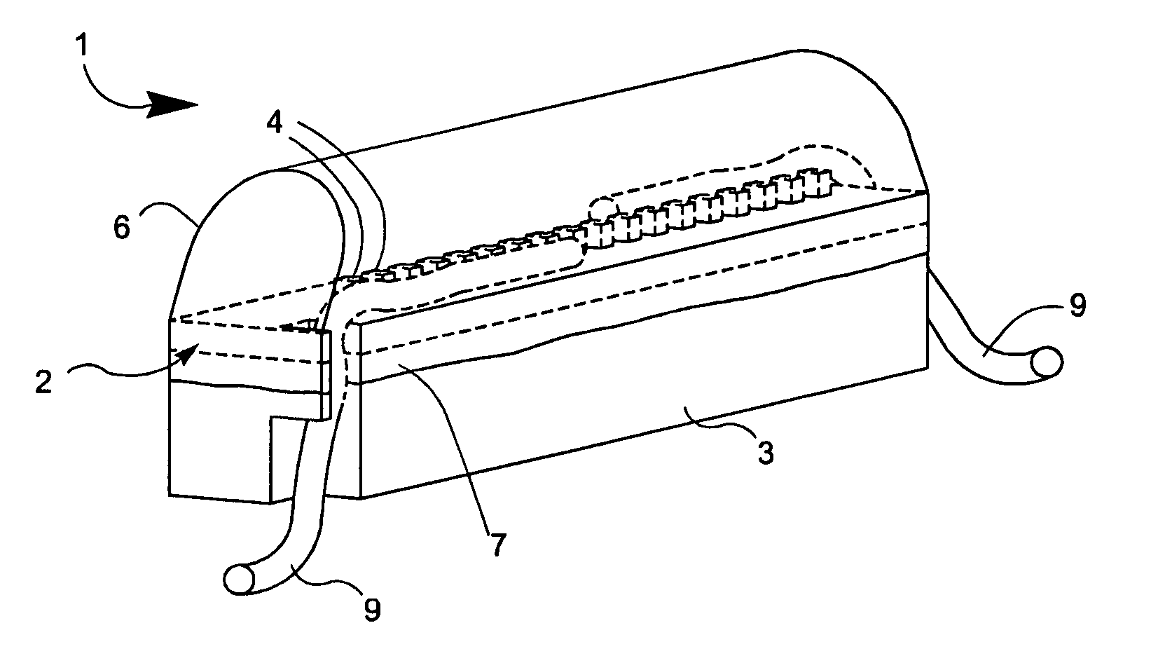
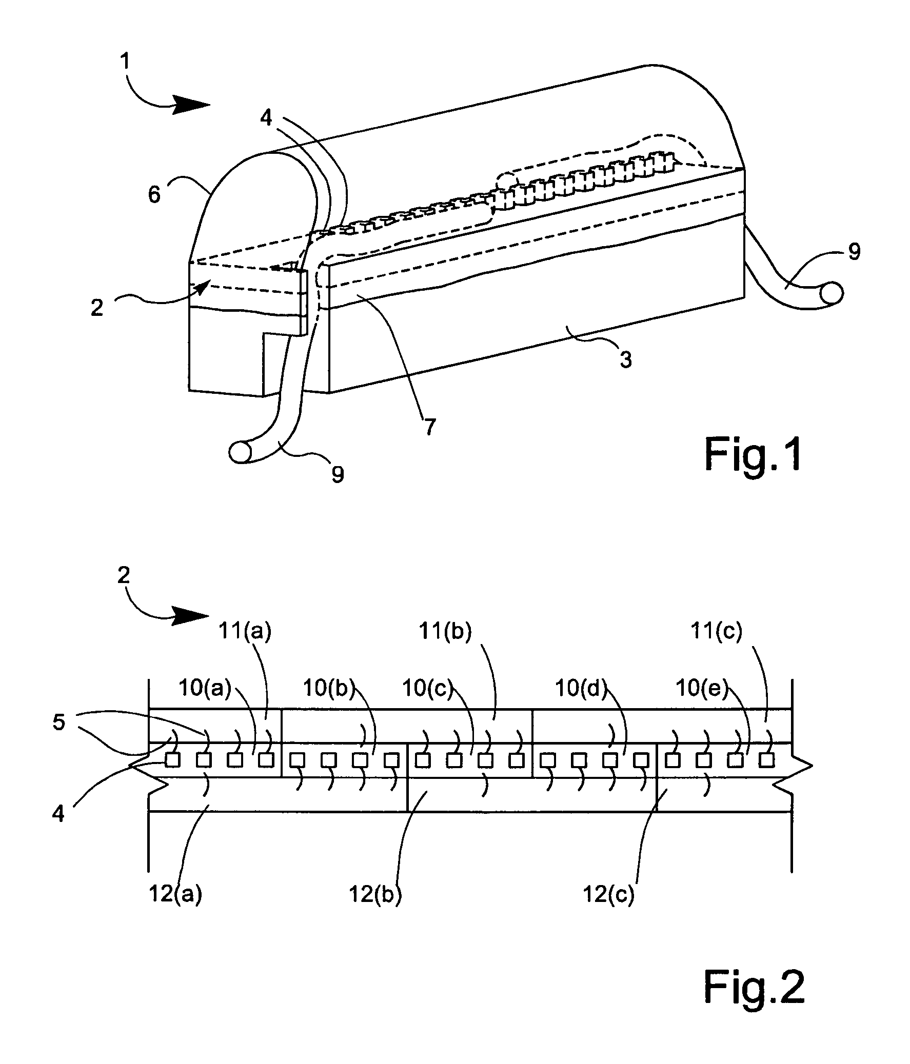
[0049]Referring to FIG. 1 an illuminator 1 is illustrated. The illuminator 1 has a linear configuration for emission of a uniform line of light on a target with a high power density. The illuminator 1 may be used alone or a number of them may be mounted together in a desired configuration according to the application.

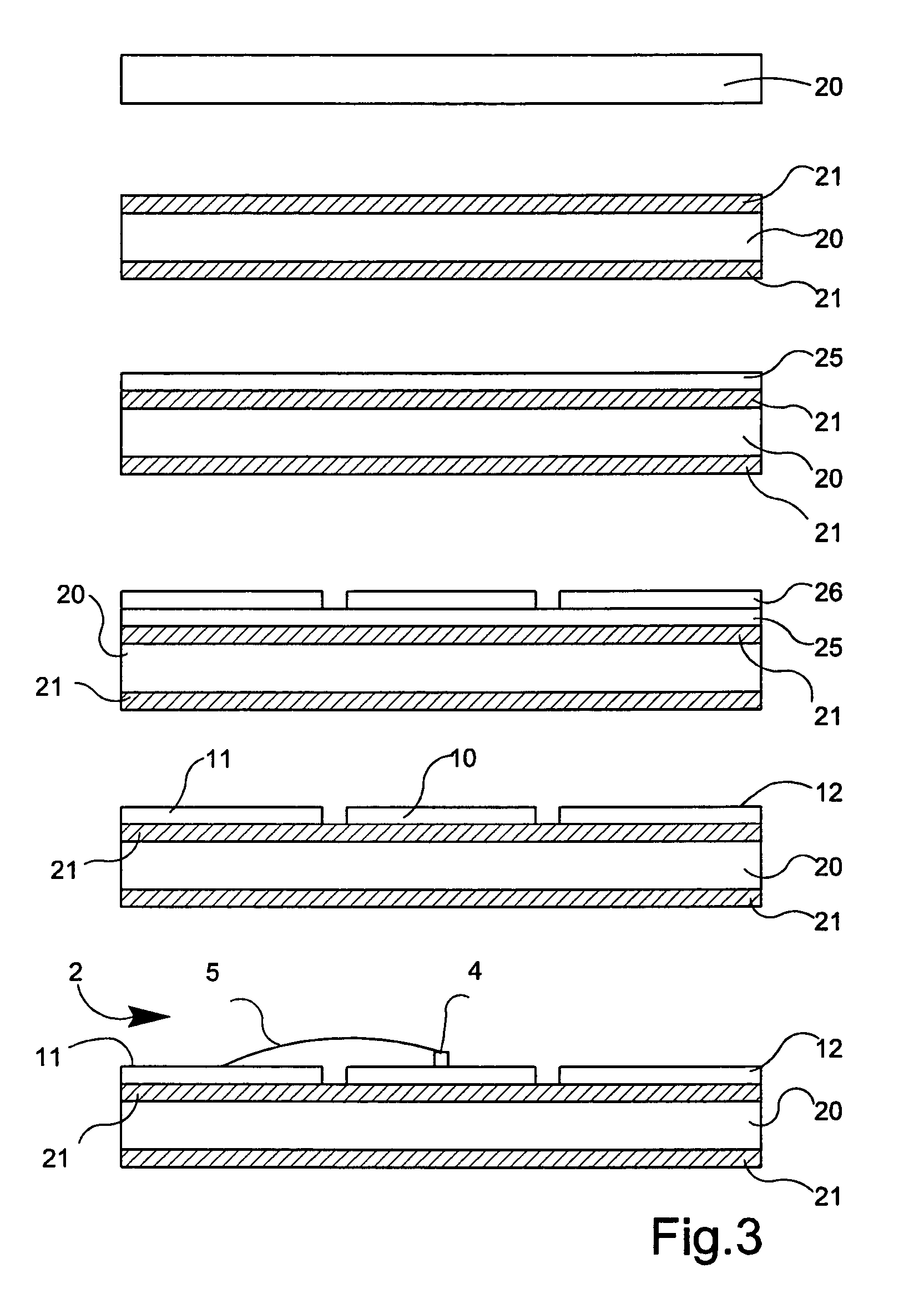
[0050]The illuminator 1 comprises a planar substrate 2 mounted on a brass heat sink 3 of rectangular block shape. The substrate 2 supports a line of light emitting semiconductor die 4 and bond wires 5 for activation. A semi-elliptical body 6 of transparent epoxy is moulded over the substrate 2 and it overlaps the sides of the substrate 2 and the top of the heat sink's sides to form an hermetic seal. The overlapping portion is indicated by the numeral 7.

[0051]As shown in FIG. 2 the substrate 2 comprises a series of central tri-metal pads 10(a), 10(b), 10(c), and 10(d). There are also a series of lateral wire bond tri-metal pads 11(a), 11(b), and 11(c) on one side and a s...


PUM


Abstract

An illuminator (1) comprises a substrate (2) supporting light source dies (4) driven via wire bonds (5). The substrate (2) comprises a silicon strip (20) in direct contact with a brass heat sink (3), thus providing for excellent heat transfer away from the die (4). Pads (10, 11, 12) of Ni, Ti, and Ag sub-layers support the die (4) and the wire bonds (5). These both provide electrical connections for the die (4) and also light reflection upwardly because the Ag sub-layers of the pads (10, 11, 12) are evaporated over a thermally grown oxide layer (21) on the Si (20). The oxide has a very high dielectric strength, thus maintaining excellent electrical insulating properties over a large voltage range.

Description

[0001]This is a continuation of PCT / IE02 / 00053 filed Apr. 23, 2002 and published in English.FIELD OF THE INVENTION[0002]The invention relates to illuminators for applications such as machine vision systems.PRIOR ART DISCUSSION[0003]Illuminators based on light emitting diodes (LEDs) are widely used for machine vision, sensing, alignment, medical, sorting, ambient lighting and other applications. For many applications such as line sources, backlights and ring lights, attributes of high power density and uniformity at the target are desirable.[0004]Such attributes are not readily available from LEDs. These are grain sized die of semiconductor material which emit light when an electric current is passed through the device. The light emitted from an LED die is highly non-directional, being quasi-isotropic, and is spatially non-uniform in radiant intensity (defined as the radiant flux emitted per space angle, W / sr).[0005]In one prior approach, to address the problems of non-directionality...

Claims


Application Information

Patent Timeline
Patent Type & Authority Patents(United States)
IPC IPC(8): H01L29/18H01L29/22H01L29/24H01L33/00H01L25/075H01L33/64
CPCH01L25/0753H01L33/64H01L33/648H01L2224/48091H01L2924/00014
Inventor BRADDELL, JULESKAVANAGH, KIERANHERBERT, ANTHONY
Owner LUMOS SOLUTIONS
Why Eureka
Try Eureka