Method for analyzing impurities in a silicon substrate and apparatus for decomposing a silicon substrate through vapor-phase reaction

a technology of vapor phase reaction and silicon substrate, which is applied in the direction of semiconductor/solid-state device testing/measurement, instruments, semiconductor materials, etc., can solve the problems of oxide membrane deformation, large thickness, leakage current of the device, etc., and achieve high precision analysis in a short time

Active Publication Date: 2006-02-07
MITSUBISHI MATERIALS SILICON CORP
View PDF2 Cites 4 Cited by
  • Summary
  • Abstract
  • Description
  • Claims
  • Application Information

AI Technical Summary

Benefits of technology

[0009]An object of this invention is to provide a method for highly precisely analyzing impurities present in a silicon substrate in a comparatively short time by decomposing the substrate through vapor-phase reaction without resorting to heating or pressurization.

Problems solved by technology

Metallic impurities contained in a silicon wafer cause leak current of the device to increase and the oxide membrane to degrade.
Because the method of non-pressurized decomposition requires, for decomposition, a period as long as about five to ten days, and has been regarded as impractical, interest has been directed towards the method of pressurized decomposition.
The above method based on pressurized decomposition, however, poses a number of problems: for the siliceous analysis sample to be safely decomposed into a sublimate in an atmosphere pressurized and heated, the vessel must be highly tightly sealed, and thus have walls with a considerable thickness of about 10-20 mm, particularly when the vessel is made of polytetrafluoroethylene (PTFE or Teflon(TM)).

Method used


Image

  • Method for analyzing impurities in a silicon substrate and apparatus for decomposing a silicon substrate through vapor-phase reaction
  • Method for analyzing impurities in a silicon substrate and apparatus for decomposing a silicon substrate through vapor-phase reaction
  • Method for analyzing impurities in a silicon substrate and apparatus for decomposing a silicon substrate through vapor-phase reaction

Examples


embodiment examples

[0041]Next, embodiment examples of the present invention are explained together with comparative examples.

embodiment example 1

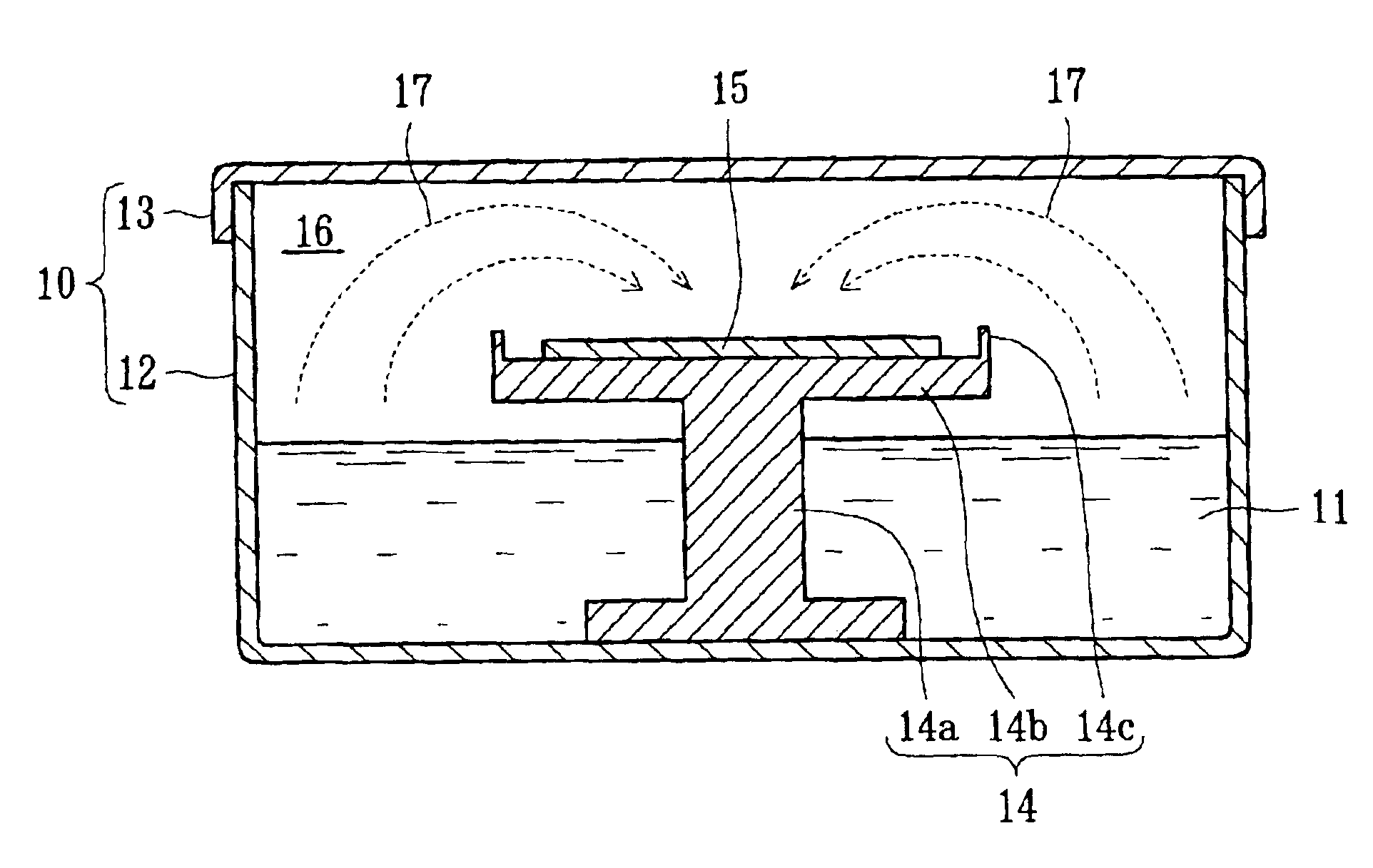
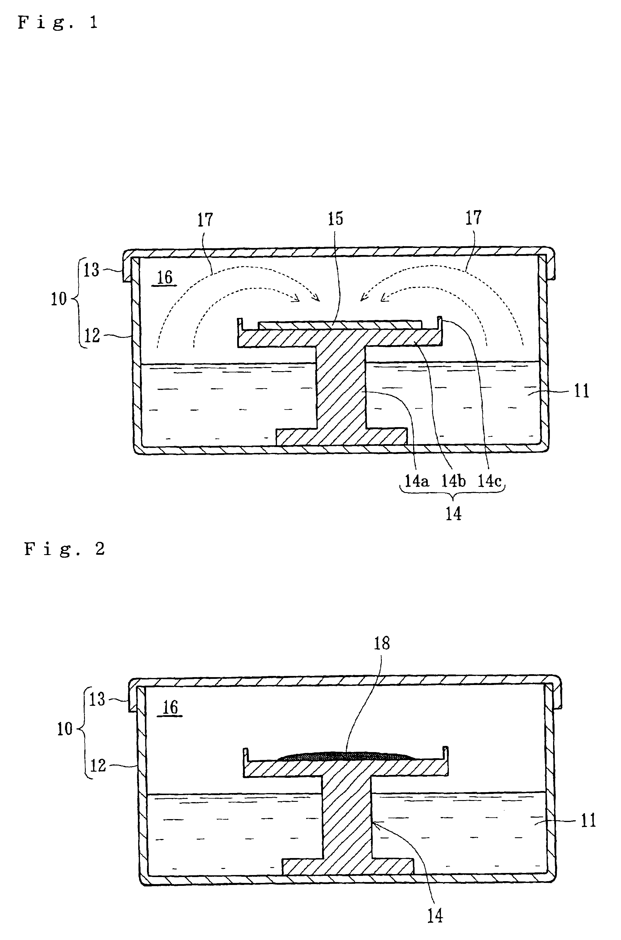
[0042]A 300 g of aqueous solution of 50 wt % HF and 200 g of aqueous solution of 68 wt % HNO3 were placed in a PP container with a volume of 250 mm (length)×250 mm (width)×150 mm (height), and mixed there. To this acid mixture was gently added 300 g of aqueous solution of 98 wt % H2SO4 to prepare a decomposing solution. The weight ratio of the three components of the mixture was HF:HNO3:H2SO4=0.77:0.7:1.52, and the mixture weighed 800 g. Then, a PTFE support was placed in the container. The platform of the support was at a level higher than the surface of decomposing solution. Five PTFE beakers were placed on the platform, and fragments of a silicon wafer each weighing about 1 g were put in four beakers, and the remaining one beaker was left empty. The fragments were prepared as follows: a silicon wafer was contaminated with Fe to give a concentration of 2×10¹³ atoms / cm2 on its surface, subjected to thermal treatment in a nitrogen atmosphere at 1000° C. for two hours, and cut into f...


PUM

PropertyMeasurementUnit
thicknessaaaaaaaaaa
thicknessaaaaaaaaaa
lengthaaaaaaaaaa

Abstract

A method for analyzing impurities present in a silicon substrate. The method includes the steps of accommodating a silicon substrate resting on a support, and a solution for decomposing a silicon substrate which comprises a mixture of hydrofluoric acid, nitric acid and sulfuric acid, in an air-tight reaction vessel, in such a way as to keep the silicon substrate from directly contacting with the decomposing solution; allowing the decomposing solution to vaporize, thereby causing the substrate to decompose through vapor-phase reaction for sublimation, without heating or pressurizing the reaction vessel; and recovering the residue left by the decomposed substrate, to analyze the impurities contained in the substrate. This method makes it possible to determine the content of impurities that are present in a silicon substrate extremely precisely in a comparatively short time by decomposing the substrate through vapor-phase reaction without resorting to heating or pressurization.

Description

BACKGROUND OF THE INVENTION[0001]1. Field of the Invention[0002]The present invention relates to a method for analyzing impurities in a silicon substrate represented by a silicon wafer, and an apparatus for decomposing a silicon substrate through vapor-phase reaction. More specifically, the present invention relates to a method for analyzing impurities in a silicon substrate without resorting to heating or pressurizing, and an apparatus for decomposing a silicon substrate through vapor-phase reaction.[0003]2. Description of the Related Art[0004]Metallic impurities contained in a silicon wafer cause leak current of the device to increase and the oxide membrane to degrade. Therefore, as the semiconductor device is more densely integrated to perform a higher function, impurities thereof come to have a greater impact on the performance of the device. To meet this situation, demand becomes acute for a method by which it is possible to directly evaluate the purity of a silicon wafer by di...

Claims


Application Information

Patent Timeline
Patent Type & Authority Patents(United States)
IPC IPC(8): G01N1/00G01N1/28G01N27/62G01N1/32G01N1/36G01N1/40G01N21/31G01N31/00G01N33/00H01L21/304H01L21/66
CPCG01N1/32G01N1/40G01N2033/0095
Inventor SHABANI, MOHAMMAD B.OKUUCHI, SHIGERU
Owner MITSUBISHI MATERIALS SILICON CORP
Why Eureka
Try Eureka