Method for verification of resolution enhancement techniques and optical proximity correction in lithography

a resolution enhancement and optical proximity correction technology, applied in the field of semiconductor device manufacturing, can solve the problems of prone to failure, failure to meet the requirements of the overall operation of the integrated circuit, and the limitation of the minimum feature size that can be accurately produced on the substra

Inactive Publication Date: 2006-02-07
IBM CORP
View PDF9 Cites 22 Cited by
  • Summary
  • Abstract
  • Description
  • Claims
  • Application Information

AI Technical Summary

Benefits of technology

[0011]In still another embodiment, a storage medium includes a machine readable computer program code for model-based verification of resolution enhancement techniques (RET) and optical proximity correction (OPC) in lithography, and instructions for causing a computer to implement a method. The method includes scaling shapes of a drawn mask layout to their corresponding intended wafer dimensions so as to create a scaled image. A first feature of the scaled image is shifted with respect to a second feature of the scaled image in accordance with a predetermined maximum overlay error. An intersection parameter of the first and said second features of the scaled image is calculated so as to determine a yield metric of an ideal layout. A first feature of a simulated wafer image of the drawn mask layout is shifted with respect to a second feature of the simulated wafer image in accordance with the predetermined maximum overlay error, wherein the first and second features of said simulated wafer image correspond to the first and second features of the scaled image. An intersection parameter of the first and said second features of the simulated wafer image is calculated so as to determine a yield metric of a simulated layout, and the yield metric of the simulated wafer image is compared to the yield metric of the scaled image.

Problems solved by technology

The minimum feature size that can be accurately produced on a substrate is limited by the ability of the fabrication process to form an undistorted optical image of the mask pattern onto the substrate, by the chemical and physical interaction of the photoresist with the developer, and by the uniformity of the subsequent process (e.g., etching or diffusion) that uses the patterned photoresist.
The inconsistent line widths can then cause circuit components that should be identical to operate at different speeds, thereby creating problems with the overall operation of the integrated circuit.
Furthermore, pulling back of the line ends can cause connections to be missed or to be weakened and prone to failure.
For example, these distortions include line width variations dependent on pattern density that affect a device's speed of operation, and line end shortening that can break connections to contacts.
Determining the optimal type, size, and symmetry (or lack thereof) is very complex and depends on neighboring geometries and process parameters.
Thus, as the gap between desired and available lithography resolution continues to widen, even more complex resolution enhancement techniques (RET) and OPC are employed to maintain profitable chip yields.
However, the task of verifying whether these complex RET and OPC solutions have achieved optimized (or even adequate) mask patterns is not a trivial endeavor.
Although simulated wafer images of RET and OPC enhanced layout shapes provide excellent qualitative insight into the patterning of certain layout shapes (and in some cases allow the extraction of quantitative information such as localized feature width or space), it is extremely difficult to guarantee that all of the millions of shapes on a given photomask will yield functional circuitry.
This is in part due to the challenge of formulating efficient, fail-safe measurements on a vast number of simulated images without drowning the output report with false nuisance errors.
Another contributing factor for making reliable ORC on large designs difficult is the ambiguous nature of the wafer target specifications.
However, many catastrophic wafer failures occur on complex two-dimensional shapes, often involving inter-level interactions that cannot be easily specified or measured on a simulated wafer image.

Method used


Image

  • Method for verification of resolution enhancement techniques and optical proximity correction in lithography
  • Method for verification of resolution enhancement techniques and optical proximity correction in lithography
  • Method for verification of resolution enhancement techniques and optical proximity correction in lithography

Examples


Embodiment Construction

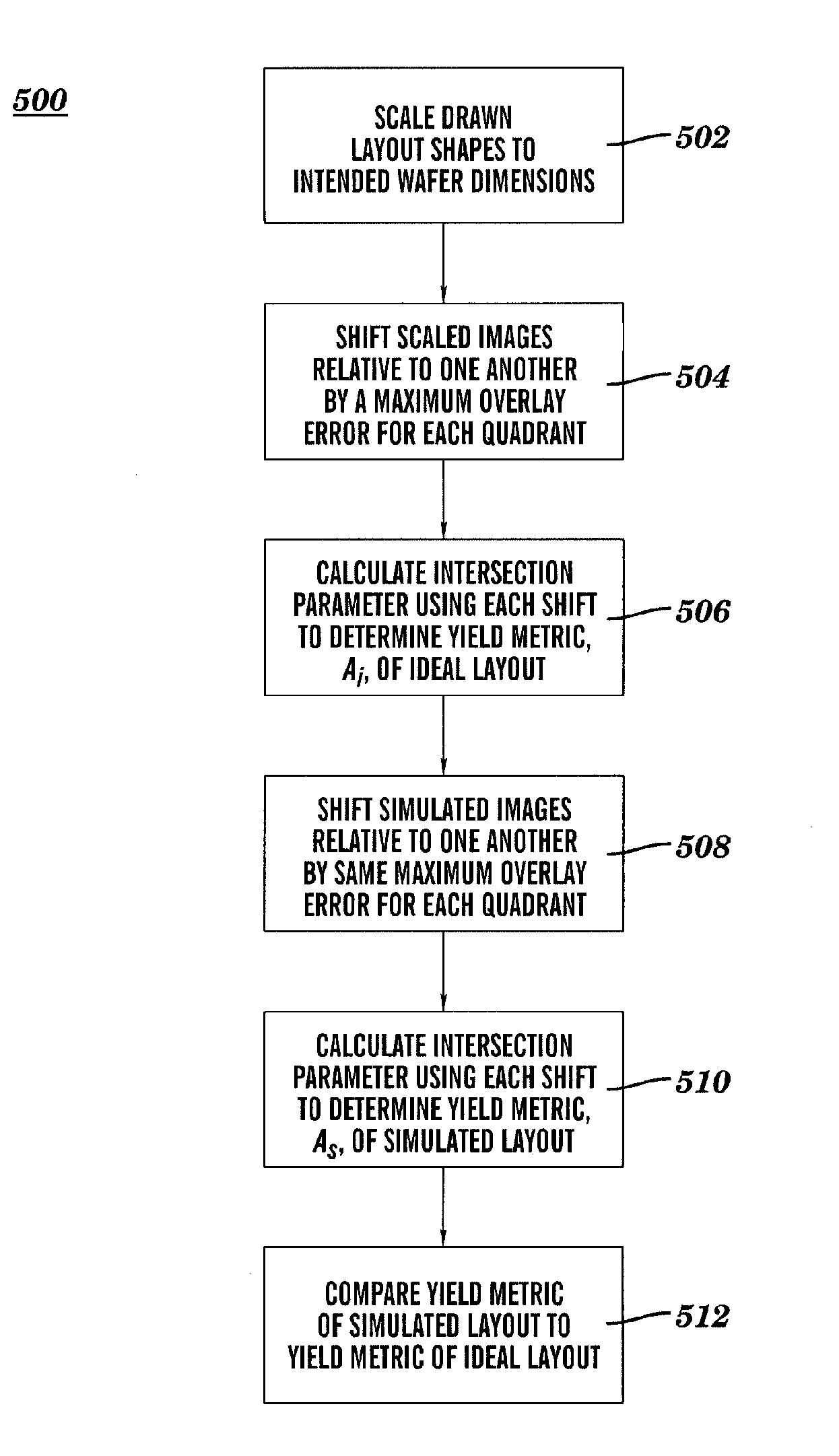
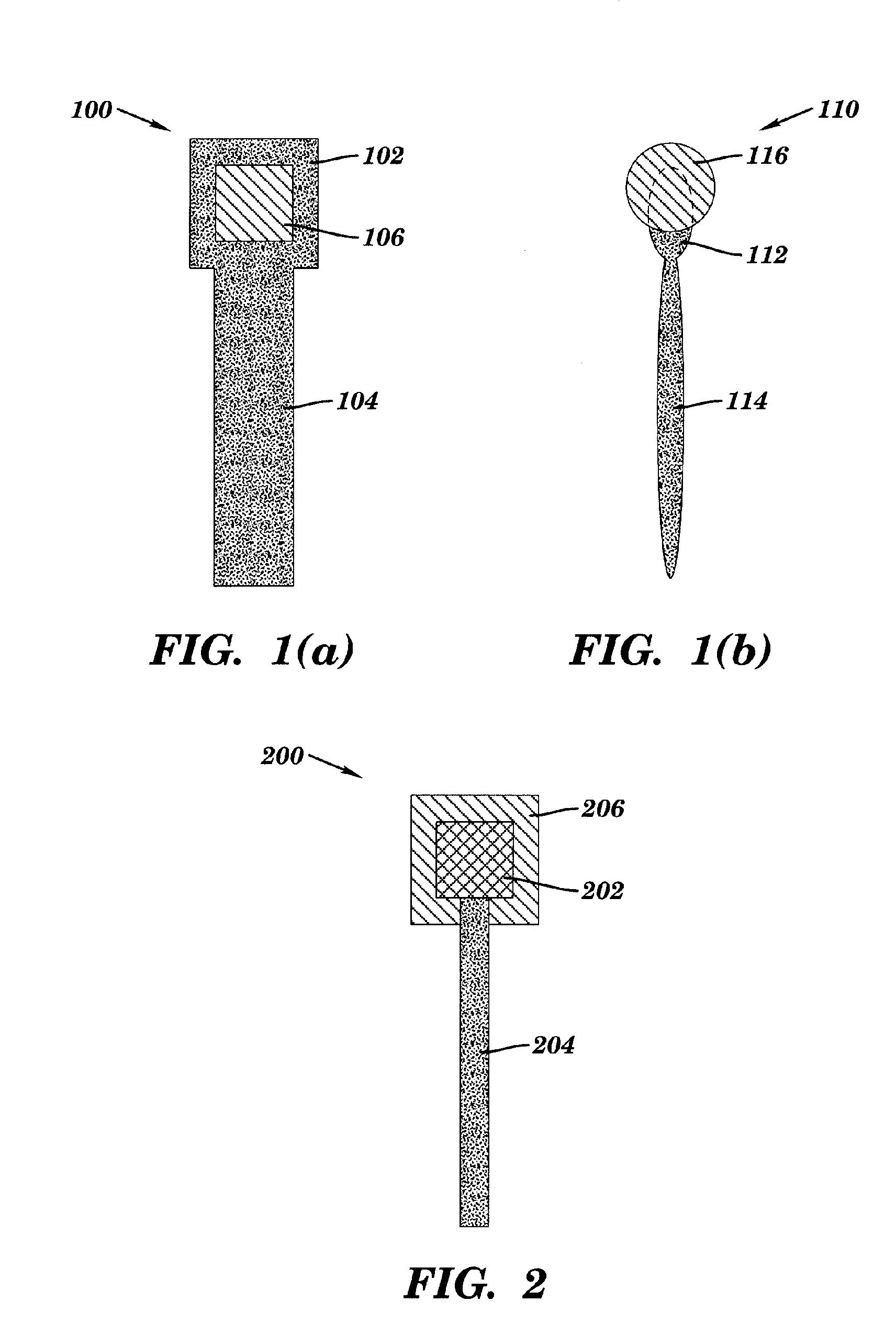
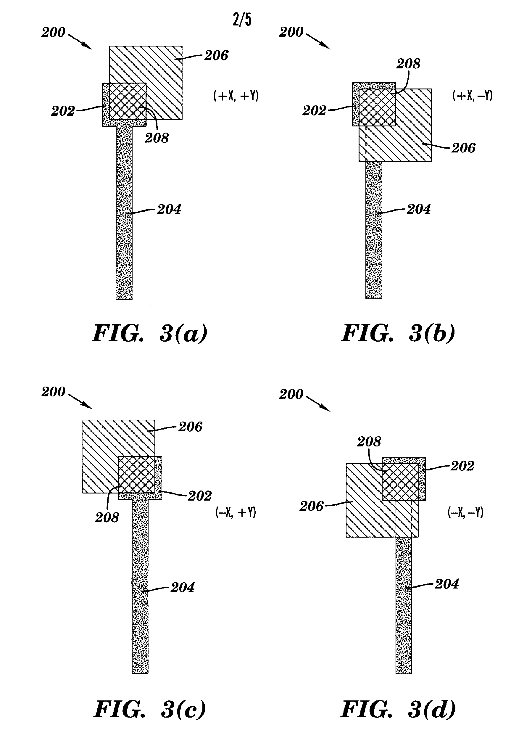
[0020]Referring initially to FIG. 1(a), there is shown a portion of an exemplary integrated circuit layout 100 featuring a poly-conductor (PC) 102 (depicted in solid) and associated conductive trace 104, along with a contact area (CA) 106 (depicted in diagonal cross hatching) for landing a connection to an upper wiring level with respect to the PC. As indicated above, when a photolithography system attempts to print circuit elements having sizes near the wavelength of the exposing radiation, the resulting shapes of the printed circuit elements become significantly different from the corresponding pattern on the mask. Accordingly, simulated wafer images of RET and OPC enhanced layout shapes have been used in an attempt to provide qualitative insight into the patterning of certain layout shapes. FIG. 1(b) thus illustrates an exemplary view of one possible simulated wafer image 110 of the design layout 100 of FIG. 1(a). As will be noted, the simulated wafer image 110 depicts the distor...


PUM


Abstract

A method for model-based verification of resolution enhancement techniques (RET) and optical proximity correction (OPC) in lithography includes scaling shapes of a drawn mask layout to their corresponding intended wafer dimensions so as to create a scaled image. A first feature of the scaled image is shifted with respect to a second feature thereof in accordance with a predetermined maximum overlay error. An intersection parameter of the first and said second features of the scaled image is calculated so as to determine a yield metric of an ideal layout. A first feature of a simulated wafer image is shifted with respect to a second feature thereof in accordance with the predetermined maximum overlay error. An intersection parameter of the first and said second features of the simulated wafer image is calculated so as to determine a yield metric of a simulated layout, and the yield metric of the simulated wafer image is compared to the yield metric of the scaled image.

Description

BACKGROUND OF INVENTION[0001]The present invention relates generally to semiconductor device manufacturing, and, more particularly, to a method and system for verification of resolution enhancement techniques and optical proximity correction in lithography.[0002]The fabrication of integrated circuits on a semiconductor substrate typically includes multiple photolithography steps. A photolithography process begins by applying a thin layer of a photoresist material to the substrate surface. The photoresist is then exposed through a photolithography exposure tool to a radiation source that changes the solubility of the photoresist at areas exposed to the radiation. The photolithography exposure tool typically includes transparent regions that do not interact with the exposing radiation and a patterned material or materials that do interact with the exposing radiation, either to block it or to shift its phase.[0003]As each successive generation of integrated circuits crowds more circuit...

Claims


Application Information

Patent Timeline
Patent Type & Authority Patents(United States)
IPC IPC(8): G06F17/50
CPCG03F1/144G06F17/5081G03F1/36G06F2217/12G06F30/398G06F2119/18Y02P90/02
Inventor LIEBMANN, LARS W.CULP, JAMES A.GRAUR, IOANA C.MUKHERJEE, MAHARAJ
Owner IBM CORP
Why Eureka
Try Eureka