Substrate for carrying a semiconductor chip and a manufacturing method thereof

a technology for semiconductor chips and substrates, applied in the field of substrates for carrying semiconductor chips, can solve the problems of increasing the difficulty of reducing the inductance between the decoupling capacitor b>14/b> and the semiconductor chip b>12/b> mounted on the substrate b>11/b>, and the difficulty of supplying stabilized electric power, particularly the supply of stabilized voltage, to the semiconductor chip. , the effect of reducing the occurren

Active Publication Date: 2006-02-14
SHINKO ELECTRIC IND CO LTD
View PDF6 Cites 32 Cited by
  • Summary
  • Abstract
  • Description
  • Claims
  • Application Information

AI Technical Summary

Benefits of technology

[0011]Another and more specific object of the present invention is to provide a chip-mounting substrate having a built-in capacitor wherein the thickness, and hence inductance, of the substrate is reduced.
[0016]According to the present invention, the capacitor is formed close to the surface on which the semiconductor chip is mounted, and the effect of inductance is minimized. Thereby, a stable power supply becomes possible from the substrate to the semiconductor chip mounted thereon. Because the capacitor, acting as a decoupling capacitor, is formed integral with the substrate, there is no need of mounting a separately manufactured capacitor on the substrate, and the process of manufacturing the semiconductor device is significantly simplified.
[0017]By forming the capacitor close to the chip-mounting surface on which a semiconductor chip is mounted, the effect of inductance on the power feeding path for feeding electric power to the semiconductor chip mounted on the substrate is minimized, and stable electric power feeding becomes possible to the semiconductor chip with stabilized voltage even in the case the clock frequency for driving the semiconductor chip is increased.
[0021]According to the present invention, the capacitor is formed integrally with the laminated structure and a built-in decoupling capacitor is obtained easily and efficiently in the laminated structure.
[0022]Particularly, it becomes possible to use a high temperature process at the time of forming the decoupling capacitor by using a baked organic polysilane film for the foregoing insulation layers. It should be noted that a baked organic polysilane film shows excellent endurance to a high temperature process. Further, by using a baked organic polysilane film for the insulation layer, the thermal expansion coefficient of the laminated structure can be adjusted to be generally equal to the thermal expansion coefficient of the semiconductor chip mounted on the substrate by controlling the baking process, and occurrence of thermal stress is minimized between the semiconductor chip and the chip-mounting surface.

Problems solved by technology

With sharp increase of clock frequency in recent advanced semiconductor devices, supply of a stable electric power to semiconductor chip is becoming a paramount problem.
In other words, the semiconductor device 10 has a drawback in that reduction of the inductance between the decoupling capacitor 14 and the semiconductor chip 12 mounted on the substrate 11 is difficult.
Associated with this drawback, there arises a problem that supply of stabilized electric power, particularly the supply of stabilized voltage, to the semiconductor chip becomes difficult because of the existence of the inductance.
This problem becomes particularly serious in recent high-speed semiconductor devices in which the semiconductor chip is driven at a very high clock speed.
Because of such a construction, the conventional semiconductor device 10 shown in FIG. 9 has suffered from the problem of complex manufacturing process and the associated problem of high manufacturing cost.
Associated with the use of such a silicon substrate, there arises a problem that a dicing process becomes necessary for separating the capacitor components 14 formed on a common silicon substrate, while such a dicing process also increases the cost of the substrate 11.
Further, associated with the use of silicon substrate for the silicon film 15, there arises a problem in the semiconductor device 10 in that the decoupling capacitor 14 cannot be formed as thin as desired, and because of this, the thickness of the substrate 11 has been increased.
However, formation of such a depression 18 makes the manufacturing process and structure of the substrate 10 very complex.

Method used


Image

  • Substrate for carrying a semiconductor chip and a manufacturing method thereof
  • Substrate for carrying a semiconductor chip and a manufacturing method thereof
  • Substrate for carrying a semiconductor chip and a manufacturing method thereof

Examples


first embodiment

[First Embodiment]

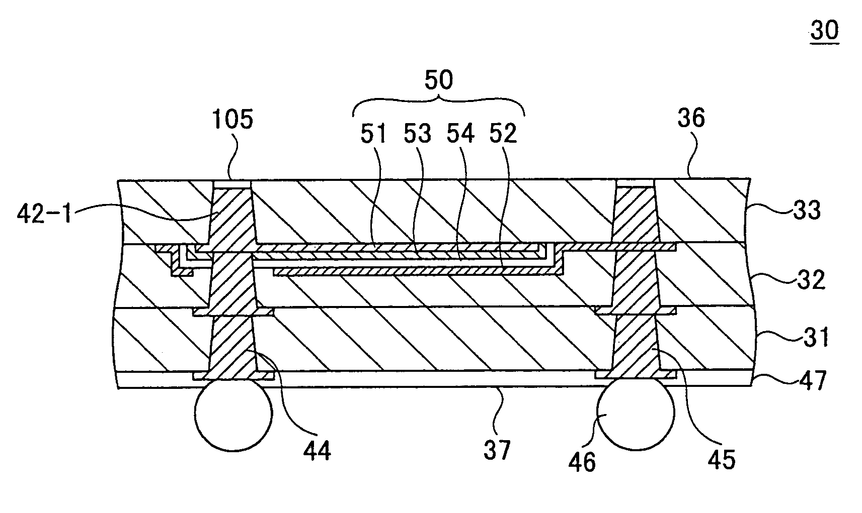
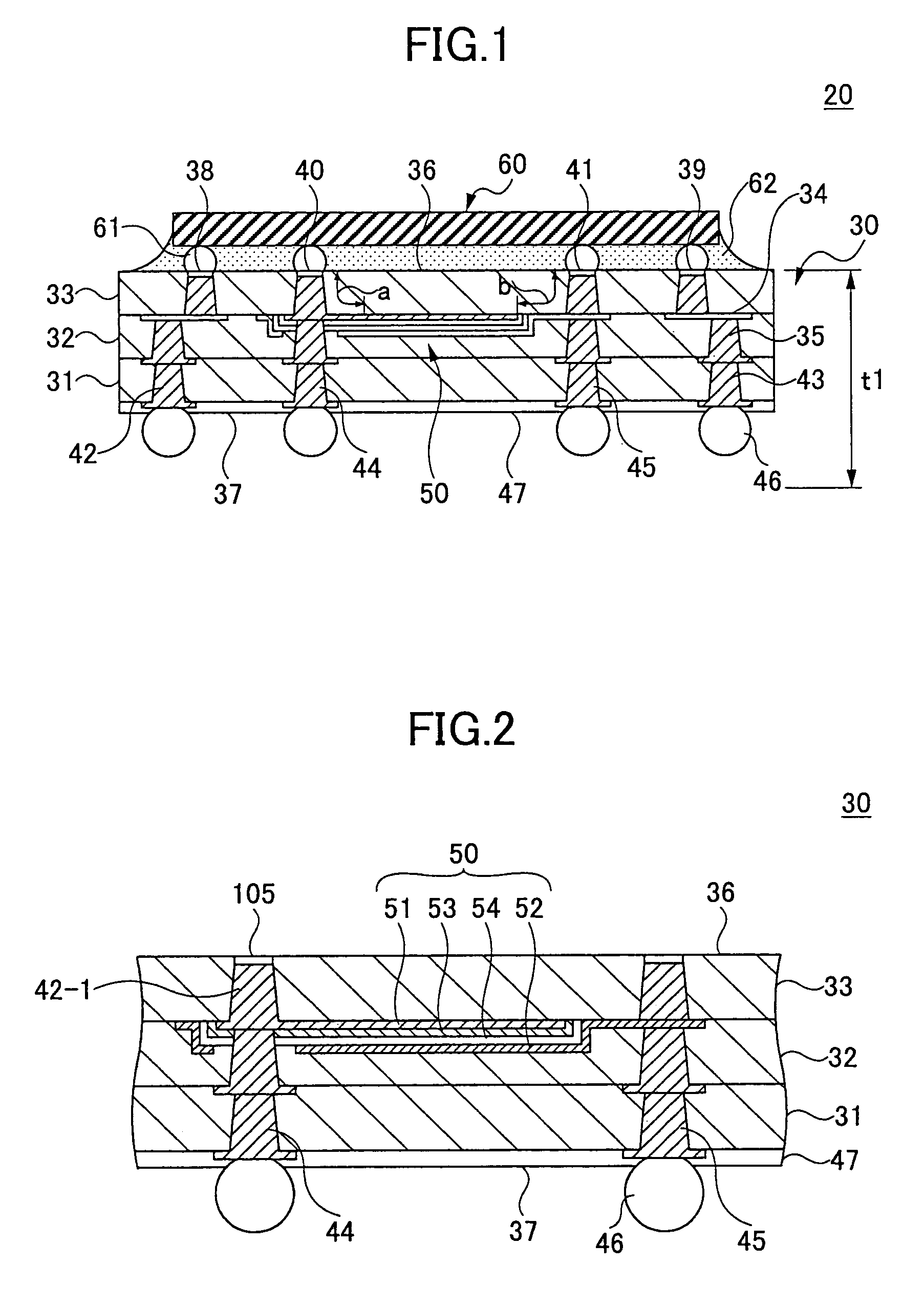
[0031]FIG. 1 shows the construction of a semiconductor device 20 according to a first embodiment of the present invention.

[0032]Referring to FIG. 1, the semiconductor device 20 is a so-called ball-grid type device and includes a semiconductor chip 60 flip-chip mounted on a chip-mounting surface 36 of a chip-mounting substrate 30 by way of bumps 61, wherein the semiconductor chip 60 is adhered to the chip-mounting substrate 30 by an underfill resin layer 62. Thereby, it should be noted that the bumps 61 on the bottom surface of the semiconductor chip 60 make an engagement with corresponding terminals exposed at the foregoing surface 36 including signal terminals 38 and 39, a power terminal 40, and a ground terminal 41.

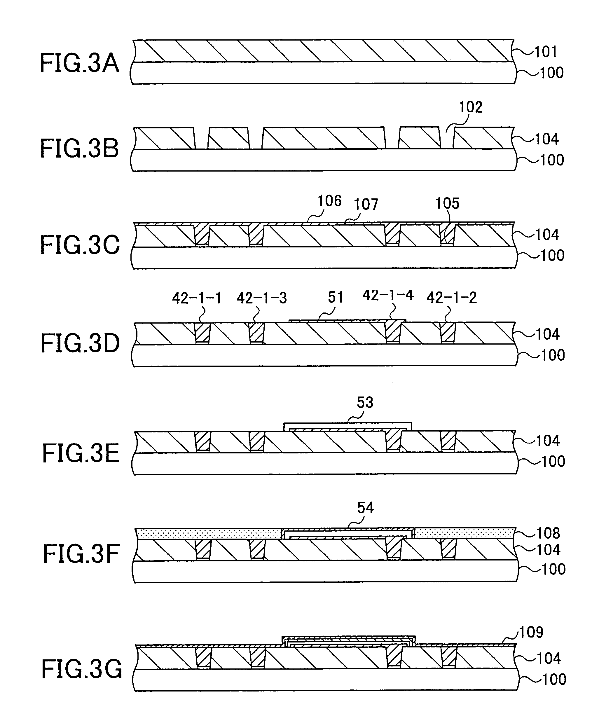
[0033]As will be explained later, the chip-mounting substrate 30 is formed by a single-side build-up process and forms a multiplayer circuit substrate including lamination of insulation layers 31, 32 and 33. The substrate 30 is defined by the foregoing...

second embodiment

[Second Embodiment]

[0080]FIG. 7 shows a semiconductor device 20B according to a second embodiment of the present invention.

[0081]Referring to FIG. 7, the semiconductor device 20B has a construction similar to the semiconductor device 20 of FIG. 1 except that a chip-mounting substrate 30B is used in place of the chip-mounting substrate 30. In FIG. 7, those parts corresponding to the parts described previously are designated by the same reference numerals added with a suffix B.

[0082]As will be explained later, the chip-mounting substrate 30B is a multilayer circuit substrate formed by a both-side buildup method and thus includes, in addition to the insulation layers 33, 32 and 31 built up in the A1 direction, insulation layers 140 and 141 that are built up in the A2 direction. The chip-mounting substrate 30B has a chip-mounting surface 36B at the top side thereof and a mounting surface 37 at the bottom surface thereof.

[0083]Similarly as before, the decoupling capacitor 50 is formed be...


PUM


Abstract

A substrate includes a plurality of insulation layers forming a laminated structure and a built-in capacitor formed in the laminated structure, wherein the laminated structure includes a layer of baked organic polysilane.

Description

CROSS-REFERENCE TO RELATED APPLICATION[0001]The present application is based on Japanese priority application No. 2002-314695 filed on Oct. 29, 2002, the entire contents of which are hereby incorporated by reference.BACKGROUND OF THE INVENTION[0002]The present invention generally relates to semiconductor devices and more particularly to a substrate for carrying a semiconductor chip and a manufacturing method thereof. Further, the present invention is related to a semiconductor device that uses such a substrate.[0003]With sharp increase of clock frequency in recent advanced semiconductor devices, supply of a stable electric power to semiconductor chip is becoming a paramount problem. In order to deal with this problem, there is a proposal to provide a capacitor on a substrate on which the semiconductor chip is mounted.[0004]FIG. 9 shows a conventional semiconductor device 10.[0005]Referring to FIG. 9, the semiconductor device 10 includes a substrate 11 mounted with a semiconductor ch...

Claims


Application Information

Patent Timeline
Patent Type & Authority Patents(United States)
IPC IPC(8): H01L21/8242H05K3/46H01L21/56H01L21/68H01L23/12H01L23/498H05K1/16
CPCH01L21/6835H01L23/49822H01L23/49894H01L21/563H01L2924/15311H01L2224/73204H01L2224/32225H01L2224/16225H05K2201/09763H05K1/162H01L2924/30105H01L2924/19041H01L23/49816H01L2221/68345H01L2221/68359H01L2924/12044H01L2924/00H01L2224/05573H01L2224/05568H01L2924/00014H01L2224/05599
Inventor OOI, KIYOSHIHORIKAWA, YASUYOSHI
Owner SHINKO ELECTRIC IND CO LTD
Why Eureka
Try Eureka