Method for manufacturing a semiconductor device

Inactive Publication Date: 2006-02-14
SEMICON ENERGY LAB CO LTD
View PDF79 Cites 91 Cited by
  • Summary
  • Abstract
  • Description
  • Claims
  • Application Information

AI Technical Summary

Benefits of technology

[0017]In the light of the aforementioned circumstances, the present invention aims to fabricate with high productivity, a thin film of crystalline silicon semiconductor by

Problems solved by technology

However, the electric characteristics of the amorphous silicon film are disadvantageously poor.
Such a heat treatment is detrimental for a glass substrate.
For instance, a Corning 7059 glass commonly used for the substrate of active matrix liquid crystal display devices has a glass distortion point of 593° C., and is therefore not suitable for large area substrates that are subjected to heating at a temperature of 600° C. or higher.
However, the presence of the catalyst elements in a large quantity in the semiconductor is

Method used


Image

  • Method for manufacturing a semiconductor device
  • Method for manufacturing a semiconductor device
  • Method for manufacturing a semiconductor device

Examples


Example

EXAMPLE 1

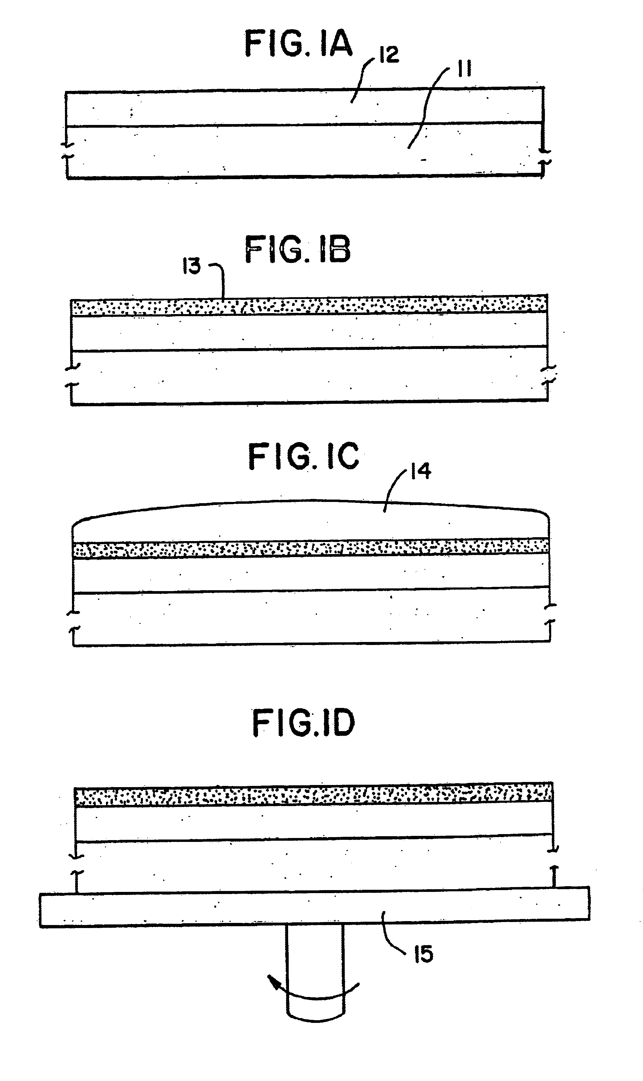
[0055]The present example refers to a process for fabricating a crystalline silicon film on the surface of a glass substrate. Referring to FIGS. 1A-1D, the process for incorporating a catalyst element (nickel in this case) into the amorphous silicon film is described below. A Corning 7059 glass substrate 100 mm×100 mm in size is used.

[0056]An amorphous silicon film from 100 to 1,500 Å in thickness is deposited by plasma CVD or LPCVD. More specifically in this case, an amorphous silicon film 12 is deposited at a thickness of 1,000 Å by plasma CVD (FIG. 1A).

[0057]Then, the amorphous silicon film is subjected to hydrofluoric acid treatment to remove impurities and a natural oxide formed thereon, if necessary. This treatment is followed by the deposition of an oxide film 13 on the amorphous silicon film to a thickness of from 10 to 50 Å. A natural oxide film may be utilized as the oxide film. The precise thickness of the oxide film 13 is not available because the film is extrem...

Example

EXAMPLE 2

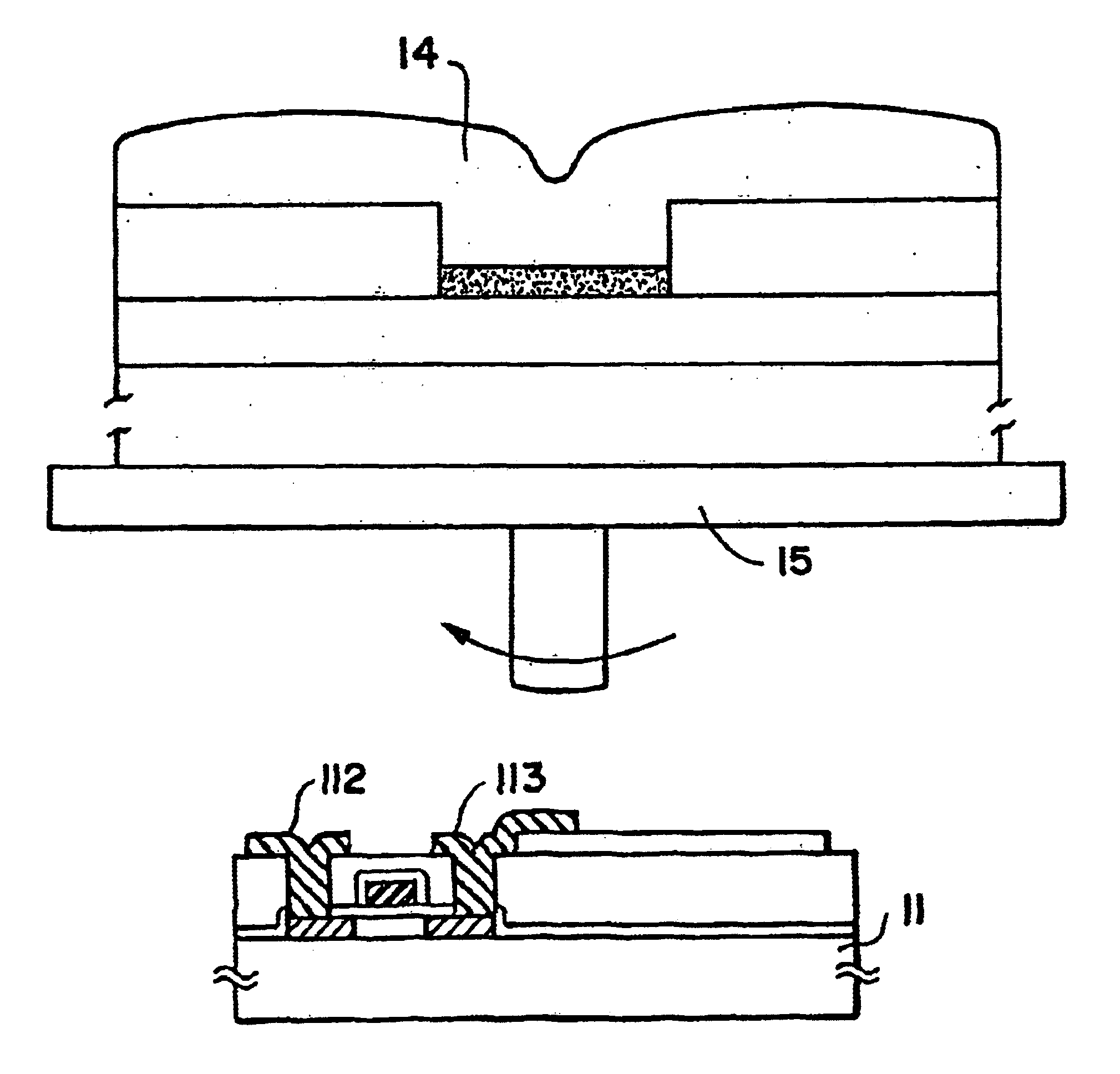
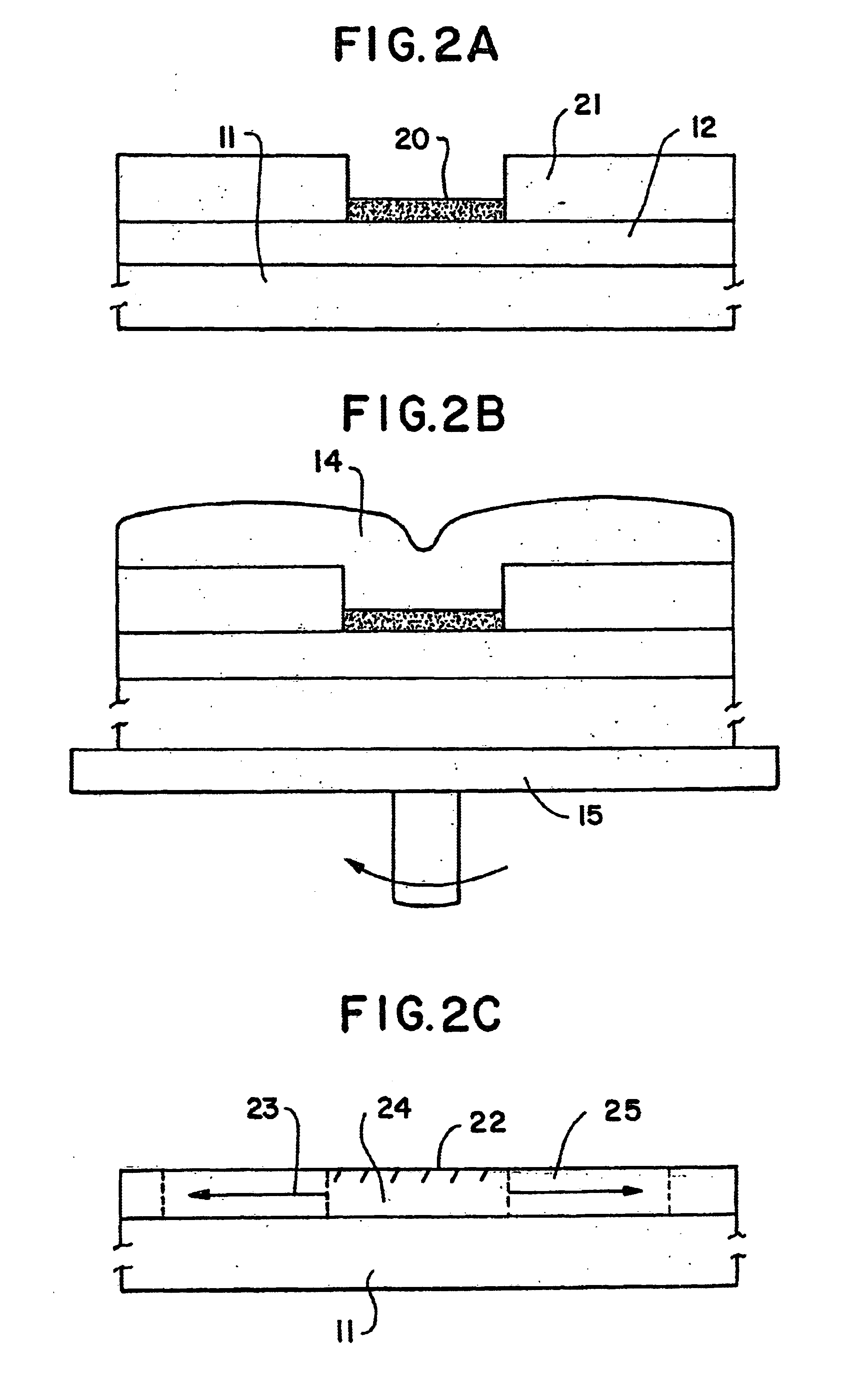
[0065]The present example refers to a process similar to that described in Example 1, except that a silicon oxide film 1,200 Å in thickness is provided selectively to incorporate nickel into selected regions of the amorphous silicon film using the silicon oxide film as a mask.

[0066]Referring to FIGS. 2A to 2C, the process for fabricating a semiconductor according to the present example is described below. A silicon oxide film is deposited to a thickness of 1,000 Å or more e.g. 1200 Å as a mask on an amorphous silicon film 12. The silicon oxide film 21, however, may be thinner than 1000 Å, e.g. 500 Å if the film is sufficiently dense as a mask. The silicon oxide film 21 is patterned into a predetermined pattern thereafter by means of a conventional photolithography technique. A thin silicon oxide film 20 is formed by irradiating a UV radiation in oxygen atmosphere for 5 minutes. The thickness of the silicon oxide film 20 is presumably from about 20 to 50 Å (FIG. 2A). The fun...

Example

EXAMPLE 3

[0091]The present example relates to a process for fabricating TFTs which are provided to each of the pixels of an active matrix liquid crystal display device, using a crystalline silicon film fabricated by the process according to the present invention. The TFTs thus obtained can be applied not only to liquid crystal display devices, but also to a wide field generally denoted as thin film integrated circuits (ICs).

[0092]Referring to FIGS. 6A to 6E, the process for fabricating a TFT according to the present example is described below. A silicon oxide film (not shown in the figure) is deposited to a thickness of 2,000 Å as a base coating on a glass substrate. This silicon oxide film is provided to prevent the diffusion of impurities into the device structure from the glass substrate.

[0093]An amorphous silicon film is deposited thereafter to a thickness of 1,000 Å in a manner similar to that used in Example 1. After removing the natural oxide film by a treatment using hydrofl...


PUM

PropertyMeasurementUnit
Concentrationaaaaaaaaaa
Semiconductor propertiesaaaaaaaaaa

Abstract

A process for fabricating a highly stable and reliable semiconductor, comprising: coating the surface of an amorphous silicon film with a solution containing a catalyst element capable of accelerating the crystallization of the amorphous silicon film, and heat treating the amorphous silicon film thereafter to crystallize the film.

Description

BACKGROUND OF THE INVENTION[0001]1. Field of the Invention[0002]The present invention relates to a process for manufacturing a semiconductor device having a crystalline semiconductor. The present invention further relates to an electro-optical device such as an active matrix liquid crystal device using the semiconductor device.[0003]2. Prior Art[0004]Thin film transistors (referred to simply hereinafter as “TFTs”) are well known and are widely used in various types of integrated circuits or an electro-optical device, and particularly used for switching elements provided to each of pixels of an active matrix(-addressed) liquid crystal display device as well as in driver elements of the peripheral circuits thereof.[0005]An amorphous silicon film can be utilized most readily as the thin film semiconductor for a TFT. However, the electric characteristics of the amorphous silicon film are disadvantageously poor. The use of a thin film of polysilicon (polycrystalline silicon), which is a ...

Claims


Application Information

Patent Timeline
IPC IPC(8): H01L29/04H01L21/20H01L21/336H01L21/77H01L21/84H01L27/12H01L29/786
CPCH01L21/2022H01L27/1277H01L29/045H01L29/66772H01L29/78654H01L29/78675H01L29/78678H01L29/66757H01L27/1296Y10S148/016H01L21/02422H01L21/02532H01L21/02672H01L21/02686H01L21/20
Inventor OHTANI, HISASHIMIYANAGA, AKIHARUFUKUNAGA, TAKESHIZHANG, HONGYONG
Owner SEMICON ENERGY LAB CO LTD
Why Eureka
Try Eureka