Memory cell with a perovskite structure varistor

a memory cell and varistor technology, applied in semiconductor devices, digital storage, instruments, etc., can solve the problems of inability to evaluate the current value at the time of the read operation, and inability to raise the degree of integration of the array serving as a memory device. achieve the effect of high integration

Inactive Publication Date: 2006-02-14
SAMSUNG ELECTRONICS CO LTD
View PDF11 Cites 50 Cited by
  • Summary
  • Abstract
  • Description
  • Claims
  • Application Information

AI Technical Summary

Benefits of technology

[0014]In consideration of these circumstances, an object of the present invention is to provide a memory cell comprising a variable resistor serving as a memory element and having a resistance body made of a thin-film material (for example, PCMO) or the like having a perovskite structure, and to provide a memory device comprising the memory cells. The memory cell comprising this variable resistor serving as a memory element and the memory device comprising the memory cells can operate at a low voltage and can be highly integrated.
[0015]Furthermore, another object of the present invention is to provide a memory device equipped with memory peripheral circuits causing no leak currents to flow to adjacent memory cells when a memory cell is accessed.
[0021]In the present invention, since the memory cell comprises a variable resistor and a current controlling device for controlling a current flowing through the variable resistor, a memory cell having a simple structure can be obtained, whereby a memory cell suited for a large-capacity memory device can be attained.

Problems solved by technology

In addition, since the voltage applied to this CMR thin film is high, this thin film is not suited for memory devices that are desired to operate at a low voltage.
Hence, the characteristics of the thin-film material can be evaluated, but there is a problem of being unable to raise the degree of integration of the array serving as a memory device.
However, leak current paths to memory cells adjacent to a memory cell to be accessed are made, whereby the current value at the time of the read operation cannot be evaluated correctly (read disturb).
Furthermore, at the time of the write operation, leak currents to adjacent cells also generate, thereby causing danger of being unable to carry out the write operation correctly (write disturb).

Method used


Image

  • Memory cell with a perovskite structure varistor
  • Memory cell with a perovskite structure varistor
  • Memory cell with a perovskite structure varistor

Examples


embodiment 1

[Embodiment 1]

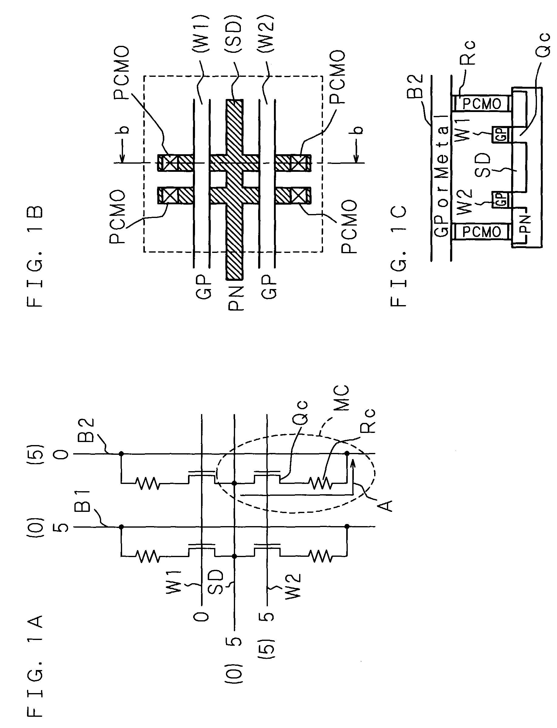
[0069]FIGS. 1A to 1C are explanatory views showing the configuration of a memory device (memory cells and a memory array) in accordance with the present invention. FIG. 1A is a circuit diagram of the memory array in accordance with the present invention. FIG. 1B is a schematic plan view showing the layout pattern of FIG. 1A. FIG. 1C is a schematic sectional view taken on arrow bb of FIG. 1B. In FIG. 1C, oblique lines indicating a sectional plane are omitted (this omission is also applicable to other sectional views).

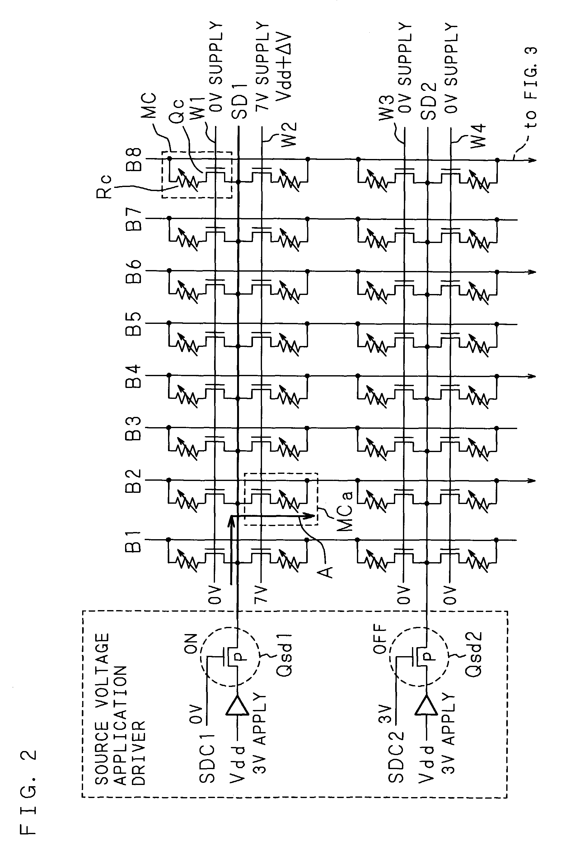
[0070]MC designates a memory cell (hereafter also referred to as a cell). MC is formed of a combination of a current controlling device Qc and a variable resistor Rc. A field-effect transistor (FET, hereafter also referred to as a Tr) is used as the current controlling device Qc (hereafter, the current controlling device Qc formed of a field-effect transistor is also referred to as a Tr Qc). The Tr Qc is connected in series with the current path of the vari...

embodiment 2

[Embodiment 2]

[0116]In a memory cell in accordance with Embodiment 2, a variable resistor having a resistance body made of a thin-film material PCMO or the like is used as a memory element, and a PN junction diode (hereafter referred to as a diode) is used instead of the FET in accordance with Embodiment 1. FIGS. 21A to 21C are views illustrating the configuration of a memory device (memory array) in accordance with the present invention. FIG. 21A is a schematic plan view (circuit diagram) showing a memory array in accordance with the present invention. FIG. 21B is a schematic sectional view taken on arrow bb of FIG. 21A. FIG. 21C is a schematic sectional view taken on arrow cc of FIG. 21A. The memory cell (and a memory array) is formed by using of a variable resistor as a memory element. The variable resistor has a resistance body made of a thin-film CMR material (for example, PCMO).

[0117]By forming memory cells, each comprising a diode and a variable resistor, at the intersections...

embodiment 3

[Embodiment 3]

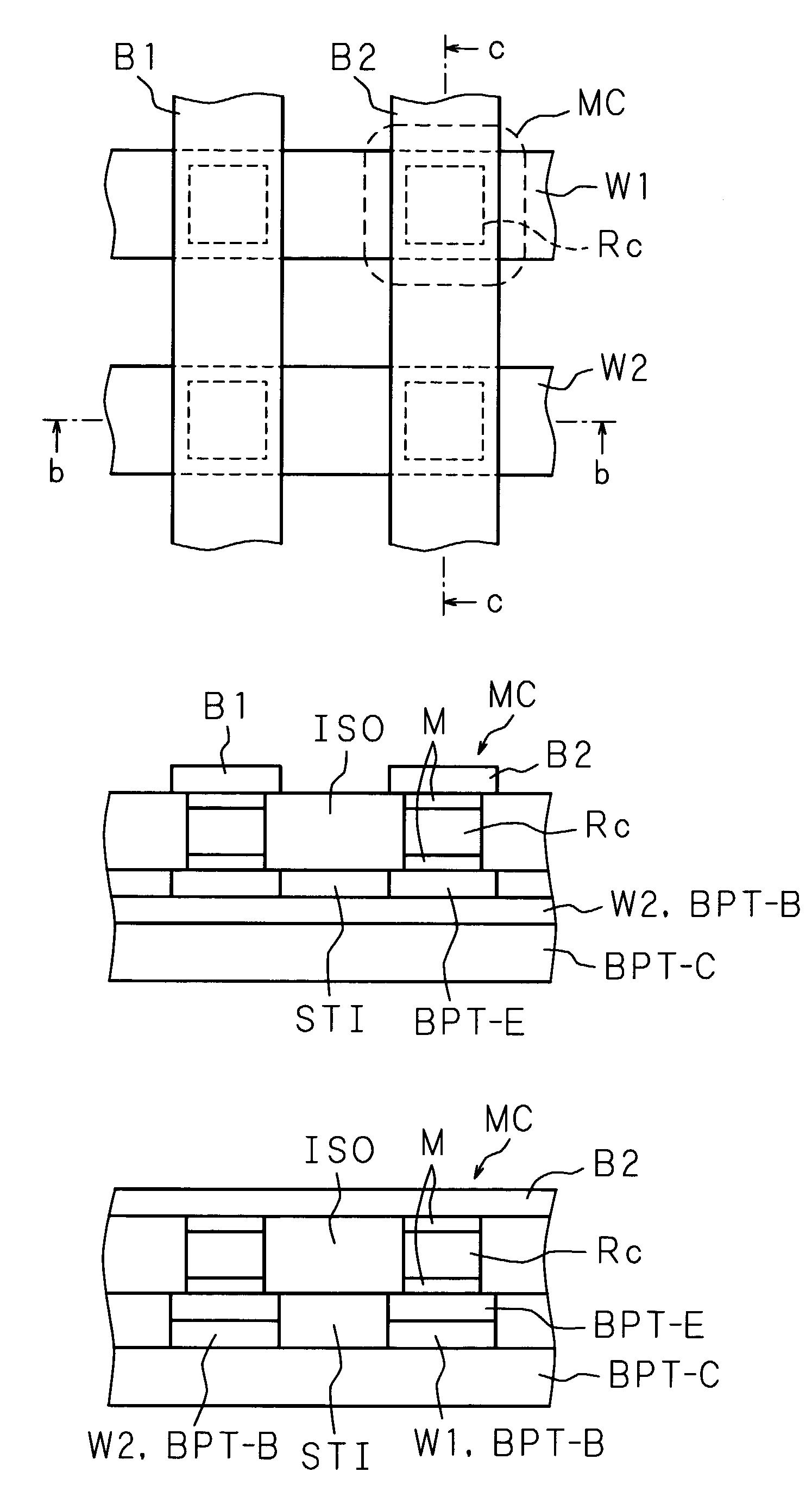
[0135]In Embodiment 1, a case wherein an FET is used as a current controlling device is shown, and in Embodiment 2, a case wherein a diode is used as a current controlling device is shown. In Embodiment 3, a case wherein a bipolar transistor (hereafter also referred to as a BPT) is used instead of an FET as a current controlling device is shown.

[0136]FIG. 35 is a view illustrating the configuration of a memory array in accordance with the present invention. The figure shows a state wherein memory cells MC are arranged in a 2 by 2 matrix to form a memory array. The memory cell MC is formed of a combination of a current controlling device Qc and a variable resistor Rc. The current controlling device Qc is formed of a BPT (hereafter, the current controlling device Qc formed of a BPT is also referred to as a BPT Qc). The BPT Qc is connected in series with the current path of the variable resistor Rc so as to control a current flowing through the variable resistor Rc. Since...


PUM


Abstract

The present invention provides a memory cell having a variable resistor as a memory element, and also provides a memory device comprising the memory cells. The variable resistor is made of a thin-film material (for example, PCMO) or the like having a perovskite structure. So the memory cell can operate at a low voltage and can be highly integrated. The memory cell MC is formed of a combination of a current controlling device and a variable resistor. A field-effect transistor, diode or bipolar transistor is used as the current controlling device. The current controlling device is connected in series with the current path of the variable resistor so as to control a current flowing through the variable resistor.

Description

BACKGROUND OF THE INVENTION[0001]The present invention relates to a memory cell and a memory device.DESCRIPTION OF THE RELATED ART[0002]A method for changing the electrical characteristics of a thin film and a bulk formed of a thin-film material having a perovskite structure, in particular, a colossal magnetoresistance (CMR) material or a high temperature superconductivity (HTSC) material, by applying one or more short electrical pulses, has been proposed. The intensity of an electric field and the current density thereof by this electrical pulse should be sufficient to change the physical state of the material and should have sufficiently low energy so as not to destroy the material. This electrical pulse may be positive or negative. By repeatedly applying a plurality of electrical pulses, the characteristics of the material can be changed further.[0003]This kind of conventional technology has been disclosed in U.S. Pat. No. 6,204,139, for example. FIGS. 29 and 30 are graphs each s...

Claims


Application Information

Patent Timeline
Patent Type & Authority Patents(United States)
IPC IPC(8): H01L29/00G11C11/15G11C13/00G11C16/02H01L21/8246H01L27/105H01L43/08
CPCG11C13/0007G11C13/0038G11C13/0069G11C2213/79G11C2013/009G11C2213/31G11C2013/0071G11C11/15
Inventor INOUE, KOJIHAMAGUCHI, KOJI
Owner SAMSUNG ELECTRONICS CO LTD
Why Eureka
Try Eureka