CAM cells and differential sense circuits for content addressable memory (CAM)

a technology of differential sense and content addressable memory, applied in the field of semiconductor circuits, can solve the problems of excessive power consumption of cam design, speed limitation of wired-or-match line design, etc., and achieve the effects of improving performance, reducing power consumption, and speeding up the speed of operation

Inactive Publication Date: 2006-02-14
HUANG XIAOHUA
View PDF8 Cites 30 Cited by
  • Summary
  • Abstract
  • Description
  • Claims
  • Application Information

AI Technical Summary

Benefits of technology

[0007]The invention provides CAM cell designs having improved performance over a conventional design. The invention further provides techniques to detect the signal (or voltage) on a match line coupled to a number of CAM cells and having faster speed of operation and possibly lower power consumption.
[0008]In an aspect, a content addressable memory (CAM) cell is provided having improved performance. The CAM cell includes a memory cell operable to store a bit value and a comparison circuit configured to detect the bit value stored in the memory cell. The comparison circuit includes (1) an output transistor coupled to a match line and configured to provide a drive for the match line based on the detected bit value, and (2) a dummy transistor coupled to a dummy line. The match line and dummy line are used to detect an output value provided by the CAM cell. In an embodiment, the dummy transistor (1) has similar dimension as the output transistor, (2) is located in close proximity to the output transistor, and (3) is turned OFF during sensing operation. The dummy transistor is used to achieve low voltage swing (small signal) sensing and provides for low power and high-speed operation.

Problems solved by technology

The conventional CAM cell and CAM sensing mechanism described above, though simple in design, have several drawbacks that affect performance.
First, speed may be limited by the wired-OR design of the match line, if some speed-enhancing techniques are not employed.
Second, excessive power may be consumed by the CAM design described above.

Method used


Image

  • CAM cells and differential sense circuits for content addressable memory (CAM)
  • CAM cells and differential sense circuits for content addressable memory (CAM)
  • CAM cells and differential sense circuits for content addressable memory (CAM)

Examples


Embodiment Construction

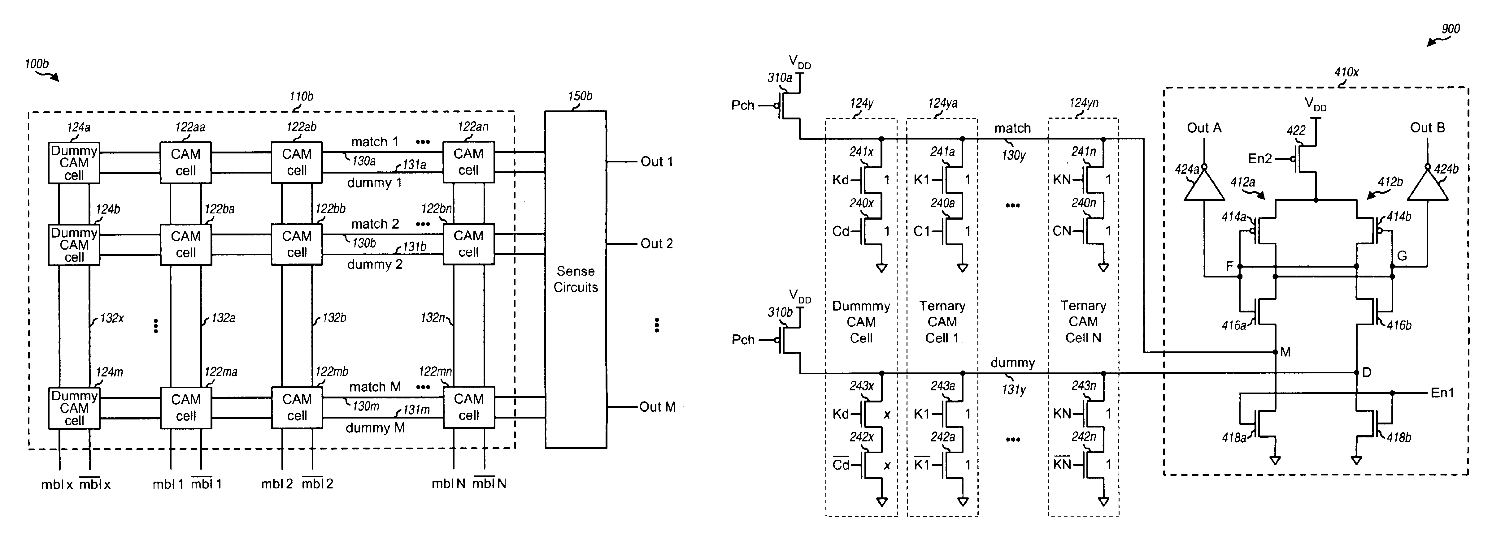
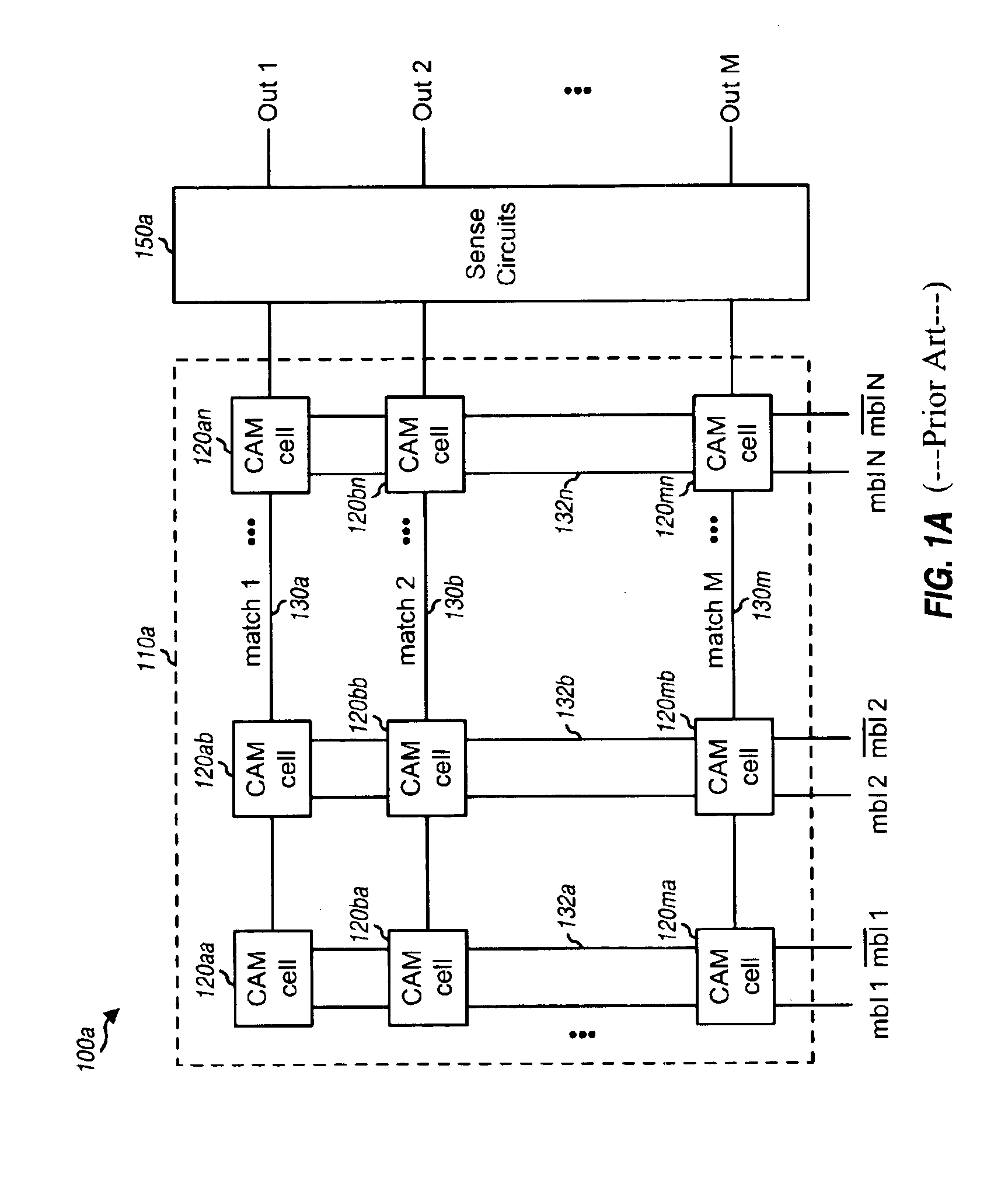
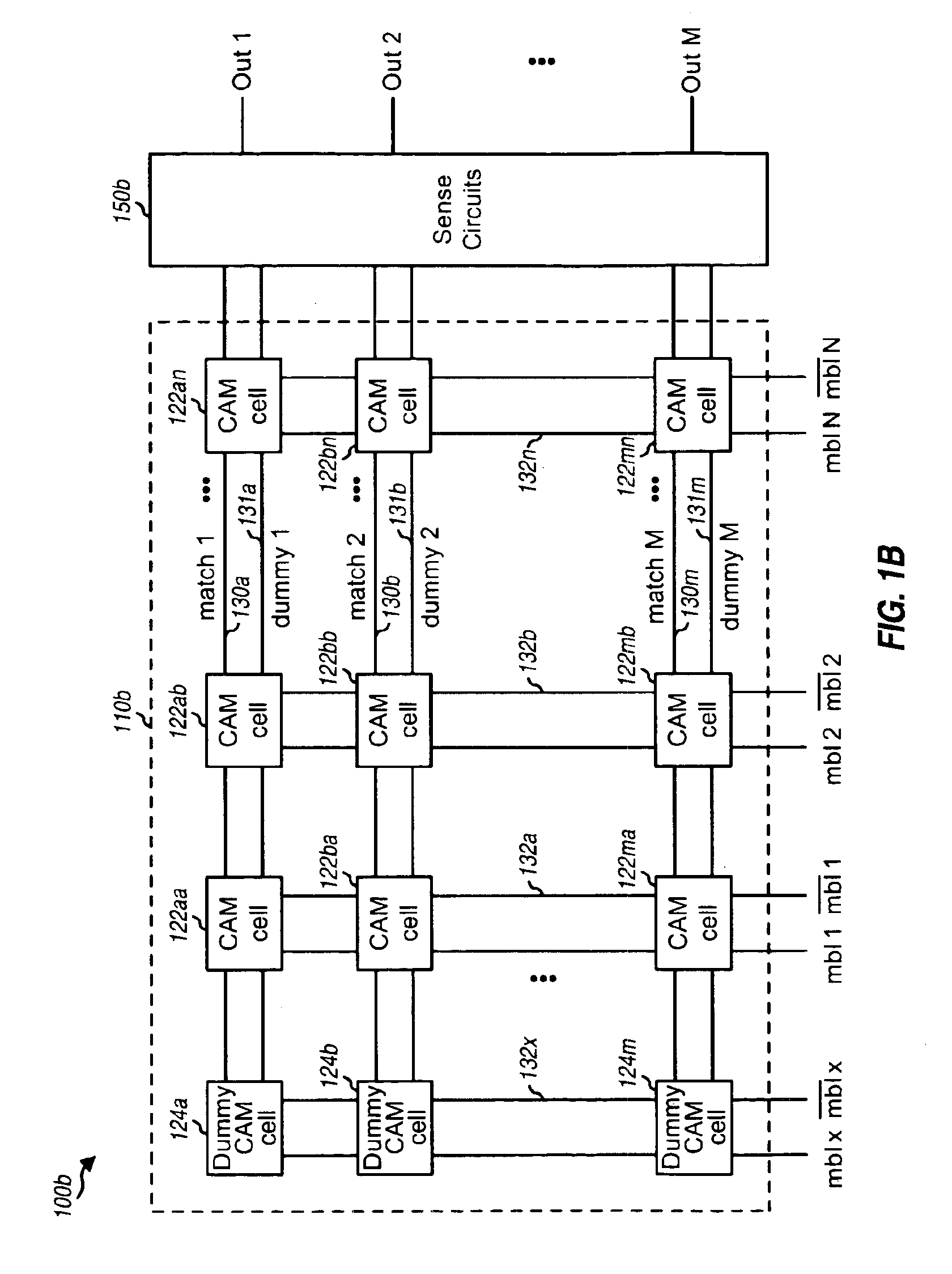
[0029]FIG. 1A is a block diagram of a conventional content addressable memory (CAM) unit 100a. CAM unit 100a includes a CAM array 110a coupled to sense circuits 150a. CAM array 110a is a two-dimensional array of M rows by N columns of CAM cells 120. Each row of the CAM array includes N cells that collectively store data for an entry in the array. Each row is further associated with a respective match line 130 that couples to all CAM cells in the row and further couples to sense circuits 150a.

[0030]Each of the N columns of the CAM array is associated with a specific bit position of an N-bit input address. A differential address line 132 is provided for each address bit and couples to all cells in the corresponding column of the CAM array. In this way, each bit of the N-bit input address may be compared with each of the M bits stored in the M cells in the corresponding column. The N-bit input address may thus be provided to all M rows of the CAM array and simultaneously compared agai...


PUM


Abstract

A dummy Content-addressable memory (CAM) cell and a dummy Ternary Content-addressable memory (TCAM) cell are connected to each row in a CAM and a ternary CAM array, respectively, to enable a differential match line sensing based on the content stored. The ternary content-addressable memory (TCAM) cell is for a differential match line sensing in low power applications. A method includes generating a voltage difference between match line signal and a reference line signal, and then detecting and amplifying the voltage difference to determine a match or a mismatch.

Description

[0001]This application is a continuation of Ser. No. 10 / 202,621 filed Jul. 24, 2002, now U.S. Pat. No. 6,744,653, which claims the benefit of provisional U.S. Application Ser. No. 60 / 327,049, entitled “High-Speed and Low Power Content Addressable Memory (CAM) Sensing Circuits,” filed Oct. 4, 2001, which is incorporated herein by reference in its entirety for all purposes.BACKGROUND OF THE INVENTION[0002]The present invention relates generally to semiconductor circuits, and more specifically to CAM cells and high speed and low power sense circuits for content addressable memory.[0003]A content addressable memory (CAM) is a memory having an array of memory cells that can be commanded to compare all or a subset of the “entries” in the array against an input address. Each entry in the CAM array corresponds to the content of the cells in a particular row of the array. Each row of the array is further associated with a respective match line, which is used as a status line for the row. All...

Claims


Application Information

Patent Timeline
Patent Type & Authority Patents(United States)
IPC IPC(8): G11C15/00G11C15/04
CPCG11C15/04
Inventor HUANG, XIAOHUA
Owner HUANG XIAOHUA
Why Eureka
Try Eureka