Quantum dots, nanocomposite materials with quantum dots, devices with quantum dots, and related fabrication methods

a nanocomposite material and quantum dots technology, applied in nanoinformatics, instruments, optical elements, etc., can solve the problems of increasing the complexity, size, and expense of high-speed electronic cores, and the rate-limiting component of oeo devices in any optical network, so as to reduce the overall fom, improve the efficiency of oeo devices, and improve the effect of performan

Inactive Publication Date: 2006-02-28
SAMSUNG ELECTRONICS CO LTD
View PDF166 Cites 186 Cited by
  • Summary
  • Abstract
  • Description
  • Claims
  • Application Information

AI Technical Summary

Problems solved by technology

Currently, the majority of optical cross-connect systems consist of high-speed electronic cores, which are complex, cumbersome, and expensive.
The complexity, size, and expense of such optical-to-electronic-to-optical (OEO) components become even more problematic with higher bit-rates and port counts, even as the cost of electronic components decreases, due to cross-talk and RF transport issues.
OEO devices are typically the rate-limiting component in any optical network.
Many all-optical switching technologies are relatively slow, and are therefore only appropriate for static configuration control.
These slow all-optical switches, however, are inadequate for fast switching applications such as dynamic packet switching (˜1 ns), header reading in packet switched networks (<25 ps), and all-optical data-processing (<1 ps).
Due to the small γ of silica, however, impractical fiber lengths (˜1000 km) are required for these devices to operate at typical telecommunication powers (˜10 mW).
While this technology is extremely advanced in the field of microelectronics, it is still in its infancy with respect to optics.
While waveguide structures have been fabricated using these techniques, they are rarely automated due to the incompatibility of the available active materials.
For instance, crystalline LiNiO3 cannot be arbitrarily inserted within a waveguide created by these techniques.
In addition, polymeric nonlinear materials, which are more easily processed, typically have χ(3) that is too low for efficient switching.
While proof-of-concept for all-optical switches based on SOAs has been shown, problems with amplified spontaneous emission buildup currently make cascading many of these switches problematic.
In addition, the materials used for SOAs (typically InP) are expensive and create inherent difficulties with coupling to standard silica fibers and waveguides.
Photonic bandgap materials are another promising approach, but manufacturing is still beyond current practical capabilities.
Finally, new nonlinear crystalline materials have been developed (e.g. periodically poled LiNbO3), but are typically expensive, and difficult to process, making incorporation into waveguide devices problematic.
Nonlinear polymers, with more appealing mechanical properties, have also been developed, but problems such as kinks in the polymer chains limit the maximum nonlinearity to a value still unsuitable for practical all-optical applications.
In cases where highly nonlinear polymers have been produced (e.g. polyacetylene), many of the appealing mechanical properties are lost, creating problems similar to those found in crystalline materials.
As such, it has been extremely difficult to find a practical material that simultaneously satisfies all of the requirements for a commercial χ(3)-based nonlinear device.
While many materials may have one or more of these desirable characteristics, at present, no single material comprises all of the optical and physical properties required for an optimal χ(3)-based optical switch.
In fact, besides SOAs, no commercial devices are currently available, primarily due to a lack of appropriate nonlinear optical materials.

Method used


Image

  • Quantum dots, nanocomposite materials with quantum dots, devices with quantum dots, and related fabrication methods
  • Quantum dots, nanocomposite materials with quantum dots, devices with quantum dots, and related fabrication methods
  • Quantum dots, nanocomposite materials with quantum dots, devices with quantum dots, and related fabrication methods

Examples


example 1

[0155]As an example of how the current invention is used, we now describe a preferred embodiment in which an engineered nonlinear nanocomposite material is incorporated into a waveguide nonlinear directional coupler. In the current example, the waveguide core is fabricated from doped silica with an index of refraction of 1.52 at 1.55 μm. It will be obvious to one of skill in the art that doped silica can have an index of refraction over a wide range of values. The current example is not meant to limit the scope of the invention, and it will be understood that variations on this example can extend to waveguides with an arbitrary index of refraction.

[0156]In the case of a nonlinear optical coupler, light is evanescently coupled between two waveguides such that a signal entering one waveguide oscillates between the two as a function of the interaction length. By choosing an appropriate length, the light can be coupled completely into one or the other of the two output waveguides. By ch...

example 2

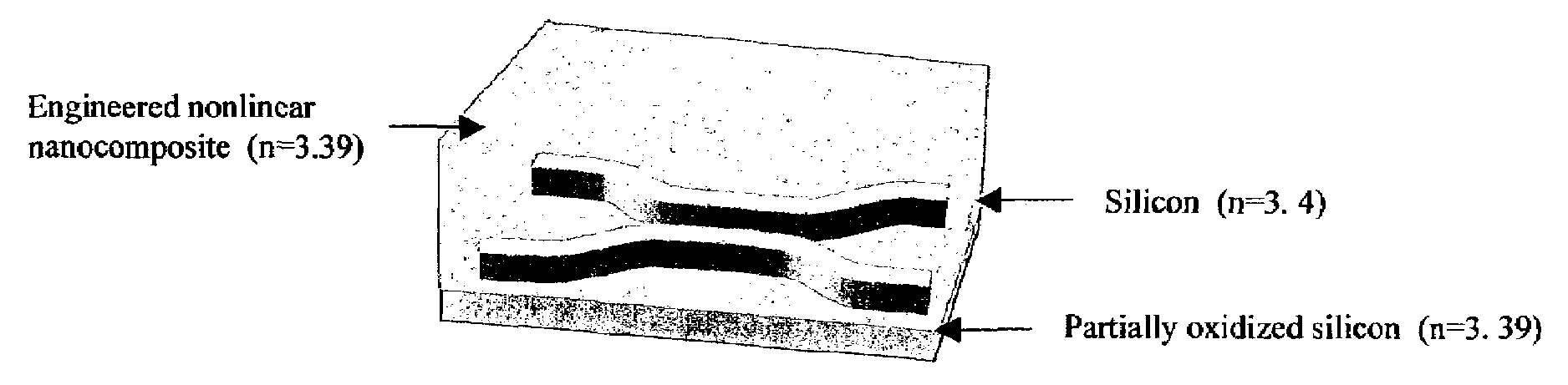
[0164]To highlight the flexibility of the current invention, a second preferred embodiment is included to demonstrate how the current invention may be used in a waveguide nonlinear Mach-Zehnder interferometer (MZI). In this case, the waveguide core is fabricated from partially oxidized silicon with an index of refraction of 2.4 at 1.55 μm. Once again, it will be apparent to one of skill in the art that partially oxidized silicon can have a range of indices of refraction, and that 2.4 is not meant to limit the scope of the invention. Variations on this example comprising other possible indices are expressly assumed and claimed under this patent.

[0165]In a nonlinear MZI, a data signal traveling along a waveguide core is split into two separate and uncoupled waveguide arms with a defined phase relation between them. The signals travel along the arms for a predetermined length and are then recombined. Phase differences resulting from the history of the light in each arm result in constr...


PUM


Abstract

The invention provides “engineered” nonlinear nanocomposite materials with an extremely large χ(3) and fast temporal response along with optical properties that can be precisely tuned to satisfy the requirements of a particular application (e.g., optical, thermal, mechanical, etc.). In particular, the magnitude of the linear and nonlinear index of refraction can be adjusted substantially independently of the absorption spectrum of the material. In addition, the optical characteristics can be engineered substantially independently from the mechanical and chemical characteristics, providing exceptional performance and flexibility in terms of device-incorporation and process-stability.

Description

CROSS-REFERENCE TO RELATED APPLICATIONS[0001]This application claims the benefit of U.S. Provisional Application Ser. No. 60 / 309,898, filed on Aug. 2, 2001, U.S. Provisional Application Ser. No. 60 / 309,905, filed on Aug. 2, 2001, U.S. Provisional Application Ser. No. 60 / 309,979, filed on Aug. 2, 2001, U.S. Provisional Application Ser. No. 60 / 310,090, filed on Aug. 2, 2001, and U.S. Provisional Application Ser. No. 60 / 310,095, filed on Aug. 2, 2001, the disclosures of which are incorporated herein by reference in their entirety.FIELD OF THE INVENTION[0002]The current invention relates to a nonlinear nanocomposite material with independently engineered optical, chemical and mechanical characteristics.BACKGROUND OF THE INVENTION[0003]As telecommunications networks continue to expand their need for bandwidth, it is becoming increasingly necessary to introduce new technologies to keep up with growing demands. These technologies must not only facilitate the need for bandwidth, but be easi...

Claims


Application Information

Patent Timeline
Patent Type & Authority Patents(United States)
IPC IPC(8): H01L31/0352
CPCB82Y10/00B82Y20/00G02B6/02195G02B6/12011G02F1/3556G02F1/3517Y10S977/834G02F3/00G02F2001/01791G02F2202/36G02F1/01791
Inventor LEE, HOWARD WING HOON
Owner SAMSUNG ELECTRONICS CO LTD
Why Eureka
Try Eureka