Display driving apparatus and display apparatus using same

a technology of display driving and display apparatus, which is applied in the direction of static indicating devices, code conversion, instruments, etc., can solve the problems of increasing the substrate area, the normal d/a conversion output cannot be achieved, and the liquid crystal display apparatus to be larger, so as to minimize the layout area, ignore the effect of voltage drop

Inactive Publication Date: 2006-02-28
SHENZHEN TOREY MICROELECTRONIC TECH CO LTD
View PDF12 Cites 36 Cited by
  • Summary
  • Abstract
  • Description
  • Claims
  • Application Information

AI Technical Summary

Benefits of technology

[0044]The present invention has an object to provide a display driving apparatus capable of realizing miniaturization of a driving circuit and reduction in power consumption of the driving circuit in a display apparatus for performing gradation display by the voltage modulation method, and the display apparatus including the same.
[0049]Likewise, it is possible to compose the second D / A converting section of switches that properly operate for input of low voltages (but cause distortion for input of high voltages), such as the NchMOS transistor and the like.
[0050]This eliminates a need of the arrangement in which one switch is composed of two transistor as in the prior art in order to attain proper operation to deal with both the high and low voltages. Thus, this reduces the number of switches (for example, transistors) to be used in D / A conversion, thereby giving a circuit for the D / A conversion a smaller layout area, thus attaining miniaturization of the display driving circuit.
[0051]Moreover, the arrangement in which the first and second D / A converting sections are respectively composed of either one type of transistors, namely PchMOS transistors or NchMOS transistors, allows the first and second D / A converting sections to be formed on separate substrates. In this arrangement, it is possible to ignore voltage drop due to back gate by appropriately setting the standard voltages that are to be supplied respectively to the first and second D / A converting sections, thereby attaining low power consumption in switching of the D / A conversion.

Problems solved by technology

Thus, if the switches of the D / A converting circuit are composed solely of either a PchMOS transistor or an NchMOS transistor, normal D / A conversion output may not be attained.
However, in the arrangement in which each one switch is composed of the two transistors, a great number of transistors are provided on a chip, resulting in an increase in a substrate area.
This gives the driving circuit a large circuit arrangement, that is, causes the liquid crystal display apparatus to be larger (in other words, this hinders miniaturizations of the liquid crystal display apparatus).
In this case, it is a problem that back gate effect due to substrate bias is caused in at least either the PchMOS transistor or NchMOS transistor, thereby causing drop in output voltage.

Method used


Image

  • Display driving apparatus and display apparatus using same
  • Display driving apparatus and display apparatus using same
  • Display driving apparatus and display apparatus using same

Examples


first embodiment

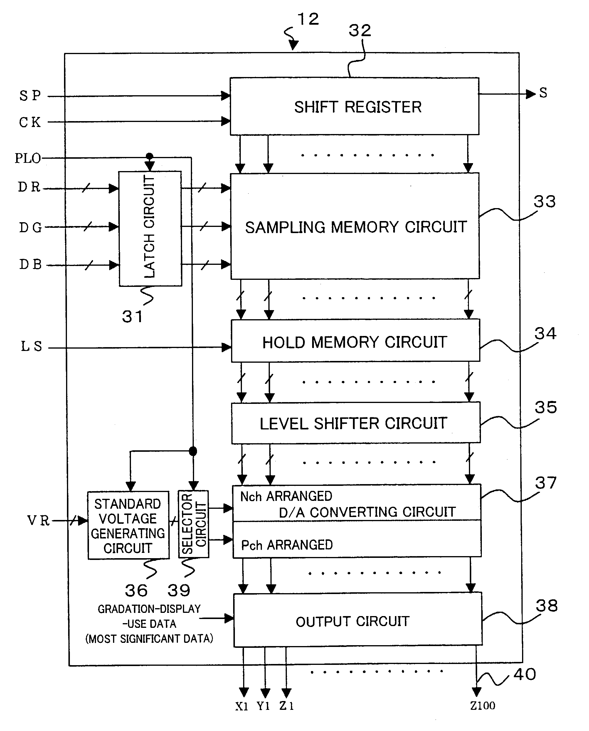
[0074][First Embodiment]

[0075]Described below is an embodiment of the present invention referring to drawings.

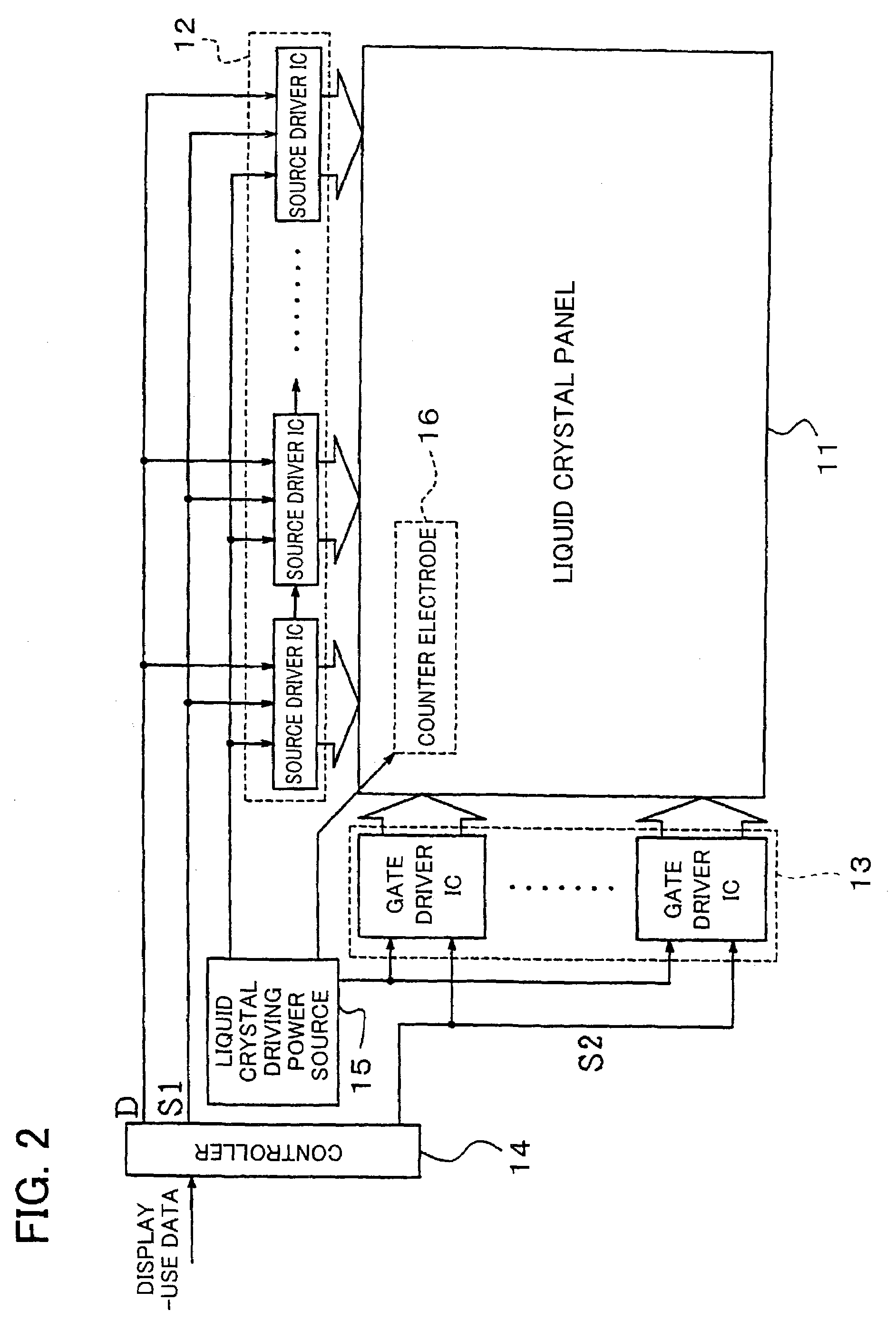
[0076]With reference to FIG. 2, a liquid crystal display apparatus of the active matrix type pertaining to the present embodiment. In the following, discussed as an example is a liquid crystal display apparatus of the TFT (Thin Film Transistor) type, which is a typical liquid crystal display apparatus of the active matrix type.

[0077]The liquid crystal display apparatus is provided with a liquid crystal display section and a liquid crystal driving apparatus for driving the liquid crystal display section. The liquid crystal display section includes a liquid crystal panel (display panel) 11 of the TFT type. In the liquid crystal pane 11, liquid crystal display elements (not shown) and counter electrodes (common electrodes) 16, which are discussed later, are provided. Meanwhile, the liquid crystal driving apparatus is provided with a source driver (display driving apparatus) 12,...

second embodiment

[0156][Second Embodiment]

[0157]Described below is another embodiment, that is, a second embodiment of the present invention.

[0158]In the source driver 12, which is the display driving apparatus of the first embodiment, the standard voltage generating circuit 36 receive the reference voltage from the outside at the terminals to receive the highest reference voltage V′64, and the lowest reference voltage V′0, so as to generate 64 levels by using the resistive divider circuit. Here, inputted as the reference voltage V′64 is a power source voltage Vcc, while GND is inputted as the reference voltage V′0. This make constant the levels of the standard voltages for displaying respective gradations, the standard voltages being outputted from the standard voltage generating circuit 36.

[0159]Moreover, in case where the display driving apparatus is adopted in a liquid crystal display apparatus for example, it is necessary to optimize the driving voltage for the liquid crystal panel in accordanc...


PUM

PropertyMeasurementUnit
polarityaaaaaaaaaa
voltageaaaaaaaaaa
standard voltagesaaaaaaaaaa

Abstract

A standard voltage generating circuit generates standard voltages as many as the number of gradations. Then, the standard voltages are separated into standard voltages of high level and those of low level, by a selector circuit, regardless of polarities thereof. One of the standard voltages of high level thus separated by the selector circuit is selected by a Pch-arranged converting section of a D / A converting circuit. Then, the selected one of the standard voltages of high level is outputted as a gradation-display-use voltage. Meanwhile, One of the standard voltages of low level thus separated by the selector circuit is selected by an Nch-arranged converting section of the D / A converting circuit. Then, the selected one of the standard voltages of low level is outputted as a gradation-display-use voltage. With this arrangement, it is possible to attain miniaturization of a circuit and lower power consumption in a display apparatus which performs gradation display by a voltage modulation method.

Description

FIELD OF THE INVENTION[0001]The present invention relates to a display driving apparatus for driving a liquid crystal panel and the like, and a display apparatus including the same, and particularly relates to a display driving apparatus, which realizes miniaturization of a driving circuit and reduction in power consumption of the driving circuit, and a display apparatus including the same.BACKGROUND OF THE INVENTION[0002]The Active matrix method is one of various display methods for a liquid crystal display apparatus. The active matrix method, which attains a very fine display, uses TFTs (Thin Film Transistor) as switching elements.[0003]In a liquid crystal display apparatus using the active matrix method, TFTs are tuned ON, line by line, in accordance with a scanning signal outputted from a gate driver. Via the TFT, a driving voltage is applied from a source driver to a pixel electrode connected to a drain of the TFT thus turned ON. Whereby, an electric charge is accumulated in a ...

Claims


Application Information

Patent Timeline
Patent Type & Authority Patents(United States)
IPC IPC(8): G09G5/10G09G3/20G02F1/133G09G3/36H03M1/76
CPCG09G3/3696G09G3/3688G09G3/3614G09G2320/0276A01K61/73E02B3/046E02B3/043
Inventor SAKAGUCHI, NOBUHISA
Owner SHENZHEN TOREY MICROELECTRONIC TECH CO LTD
Why Eureka
Try Eureka