Electrochemical device, such as an electrically controlled system with variable optical and/or energy properties

a technology of electrical control system and electrochemical device, which is applied in the direction of electrical apparatus, coatings, instruments, etc., can solve the problems of increasing the thickness of the layer a to heighten the conductivity, and achieve the effect of ensuring the continuity more effectively

Inactive Publication Date: 2006-03-14
SAINT GOBAIN VITRAGE SA
View PDF19 Cites 50 Cited by
  • Summary
  • Abstract
  • Description
  • Claims
  • Application Information

AI Technical Summary

Benefits of technology

[0035]The third version consists in combining the layer(s) of type A with a network of conducting elements, in particular based on a metal of intrinsically higher conductivity than the material of type A. Actually, as described in detail below, this network may be composed of linear elements visible to the eye at close quarters but sufficiently discreet to be compatible with most of the applications envisaged in glazing for buildings or for vehicles. It is then advantageous for these elements to be dimensioned and arranged so that their visibility is as low as possible. Generally, success can be obtained by making this network almost impossible to discern, at least when the system is in the coloured state.
[0037]The point common to these versions is that the additional conducting element, namely the material B or the network C, allows the overall electrode formed in this way to overcome a threshold of conductivity, so that the entirety of the electrode experiences the same potential difference at almost the same time as soon as the voltage is applied to the system, and this significantly reduces the switching time and reduces or even eliminates the “coloration front” effect mentioned above. And this highly interesting technical result is not obtained by compromising the optical quality of the system if:
[0041]According to the first version the layer(s) B is / are advantageously essentially metallic, in particular based on at least one noble metal or based on an alloy comprising a noble metal of the type comprising silver Ag or gold Au or copper Cu or aluminium Al. The layer selected is preferably one based on an alloy of silver with another metal, such as nickel or titanium. The reason for this is that it makes the layer much less susceptible to oxidation, in particular when it is in electrical contact with layers of electrochromic materials in an “all-solid” system. Gold is a material even less susceptible than pure silver to oxidation, but it is less satisfactory from an optical standpoint, being less neutral in transmission. The combination of a type A layer and a type B layer is of particular interest: as already seen, it allows sufficient enhancement of the electrical conductivity of type A layers with layers B which have low thickness and therefore no excessive adverse optical effect. This is also a novel means of incorporating layers B in electrodes, in particular silver layers, the use of which has hitherto posed the problem of protecting these from attack, in particular by oxidants. Thus type A layers can be used to “protect” type B layers, in particular from oxidation / degradation, the layers A having a double function as protection and electrical conductor, indeed a triple function with an added optical function when the thicknesses of the type A layers are adjusted as a function of those of the type B layers to optimize the optical appearance of the entirety by interference interaction between these different layers. It is thus possible, for example, to reduce the light reflection induced by the layer B.
[0065]Another subject of the invention is the use of the device described above for making electrochemical energy-storing devices of battery or fuel-cell type, and the batteries and cells themselves. The reason for this is that it is of very particular interest for battery applications to use the version of the invention consisting in the use of an electrode comprising a perforated metallic sheet or metallic grid. Since batteries are frequently produced on rather thin plastic substrates (of PET type, about 30 μm) if the conducting layers are flexed they are in danger of losing their electrical continuity. A thicker metallic “grid” allows this continuity to be assured more effectively.

Problems solved by technology

The reason for this is that increasing the thickness of the layer A to heighten its conductivity (i.e. lower its surface resistance) is a limited solution: firstly in terms of cost and of manufacturing time for the layer in question and secondly in terms of optical appearance: above a certain thickness layers of this type begin to absorb in the visible region.

Method used


Image

  • Electrochemical device, such as an electrically controlled system with variable optical and/or energy properties
  • Electrochemical device, such as an electrically controlled system with variable optical and/or energy properties
  • Electrochemical device, such as an electrically controlled system with variable optical and/or energy properties

Examples


example 1

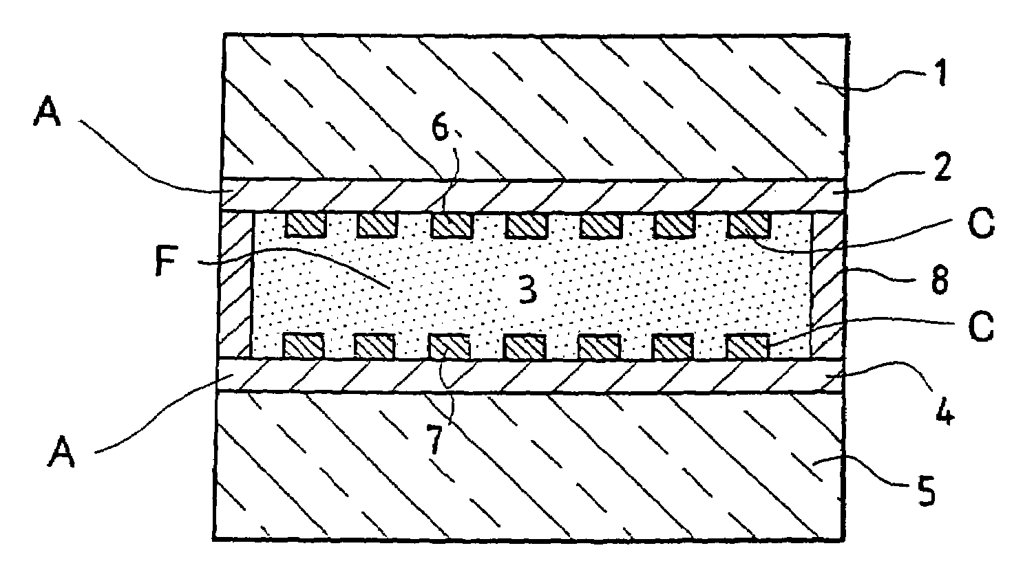
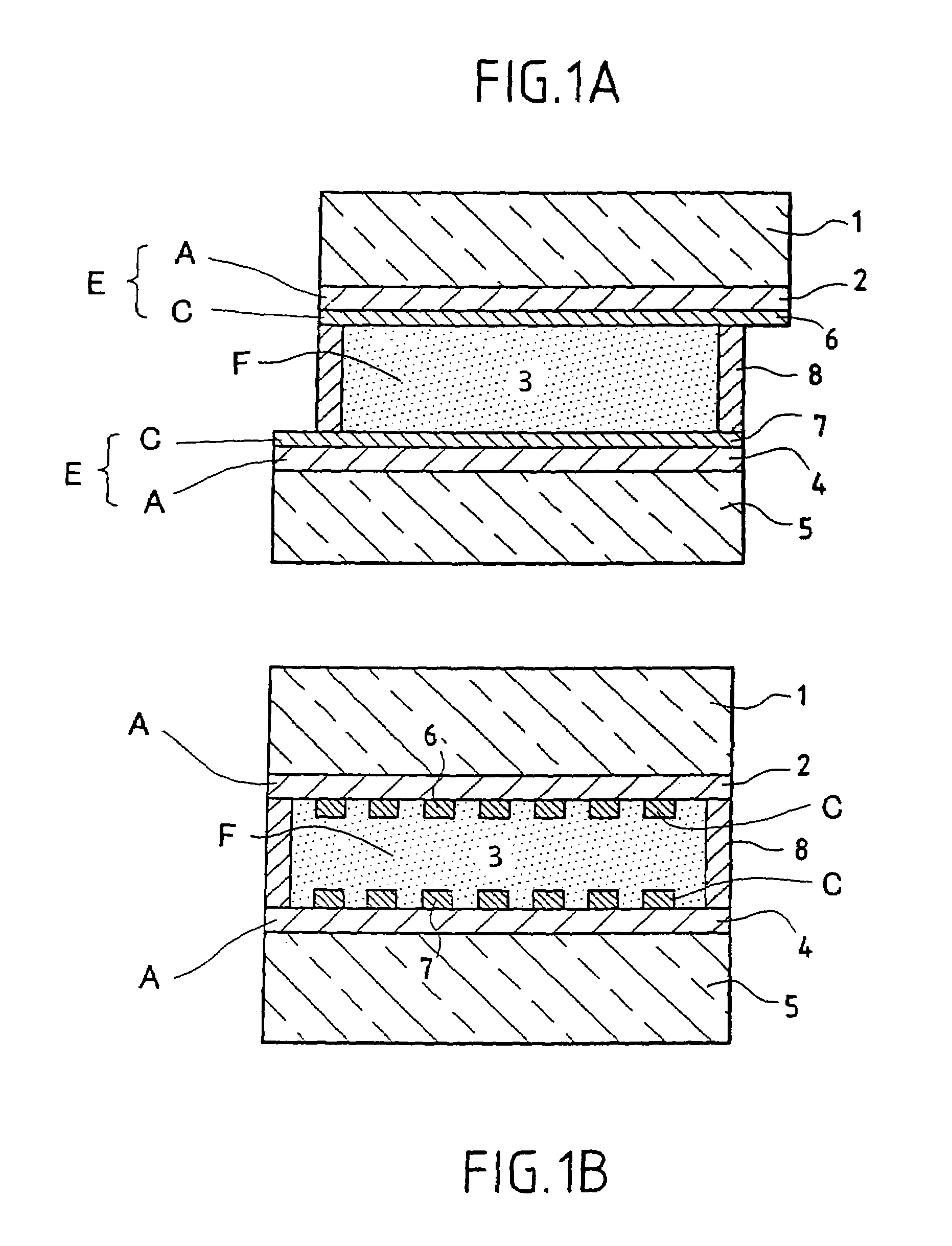
[0072]FIGS. 1a and 1b show a transverse section of a viologenic system using an “active” layer 3 of the type described in the abovementioned patent application EP-0 612 826 and based on polymer and arranged between two clear silica-soda-lime glass substrates 1 and 5 of 4 mm thickness. (FIG. 1b is a view taking a section at right angles to FIG. 1a).

[0073]The two substrates 1 and 5, each coated in advance with an SnO2:F layer 2 and 4 and laid down in a known manner by CVD have each then been provided with a network 6 and 7 of conducting strips, using a silver paste and the well known technique of screen printing. The conducting strips have a width of 0.3 mm and are essentially parallel one to the other and separated one from the other by a distance of about 2 mm. A peripheral seal 8 ensures that the system does not leak.

[0074]There are therefore two multicomponent electrodes combining a screen-printed conducting network and a doped oxide layer. The layers of SnO2:F may be replaced by ...

example 2

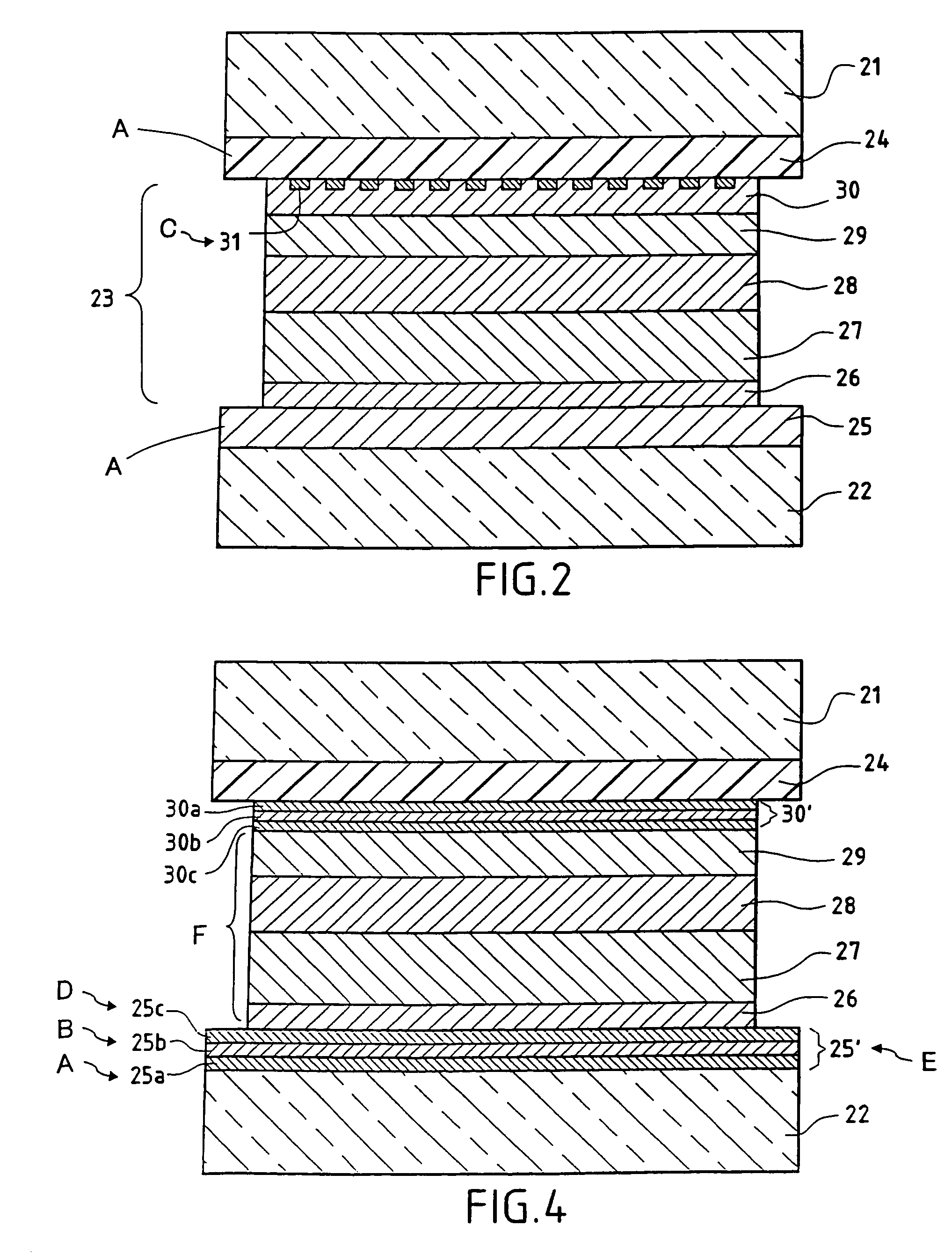
[0075]FIG. 2 represents an embodiment of electro-chromic glazing according to the invention: this is electrochromic glazing with a laminated structure and two panes of glass, in a configuration adapted, for example, for use as glazing in a car sun-roof: two clear panes of glass 21 and 22 are shown, with an electrochromic functional system 23 of “all-solid” type formed by the stack of functional layers which follows, and a sheet of polyurethane PU 24 (the sheet of PU may be replaced by a sheet of ethylene vinyl acetate EVA or of polyvinyl butyral PVB):[0076]a first 400 nm electrically conducting layer 25 of 30 SnO2:F, laid down on the glass 22 using CVD,[0077]a first 40 nm layer 26 of anodic electrochromic material made of (hydrated) iridium oxide IrOxHy (which may be replaced by a layer of hydrated nickel oxide),[0078]a 100 nm layer 27 of tungsten oxide,[0079]a second 100 nm layer 28 of hydrated tantalum oxide,[0080]a second 370 nm layer 29 of cathodic electrochromic material based ...

example 3

[0087]FIG. 4 shows another version of “all-solid” electrochromic glazing according to the invention. As in FIG. 2 and Example 2, two panes of glass 21 and 22 are seen, combined by lamination with the aid of a film 24 made of PU (or PVB: polyvinyl butyral), the layer 26 made of anodic electrochromic material, the layer 29 made of cathodic electrochromic material, these being separated by the layers 27 and 28, forming the electrolyte. By way of contrast, the electrode 25′ arranged on the glass pane 22 is now formed by a stack of layers comprising a 34 nm layer 25 (a) of SnO2 on which there is a 10 nm layer 25(b) of silver, on which there is in turn a 50 nm layer 25(c) of ITO. This three-layer structure is obtained by cathodic sputtering assisted by a magnetic field, in a known manner. The layer 25(b) of silver is optionally provided with a thin layer 25(d) of metal intended to protect it during laying down of the layer 25(c) of ITO, when this latter is laid down by a reactive method i...


PUM

PropertyMeasurementUnit
lengthaaaaaaaaaa
lengthaaaaaaaaaa
diameteraaaaaaaaaa

Abstract

An electrochemical device includes at least one carrier substrate, and a stack of functional layers including at least one electrically conducting layer that includes metal oxide(s), and a multicomponent electrode including at least one electrochemically active layer, at least one higher-conductivity material and at least one network of one of conducting wires and conducting strips. The higher-conductivity material has a surface resistance that is lower than a surface resistance of the electrically conducting layer. The stack of functional layers is arranged between two substrates, and each may be rigid, of glass type or rigid polymer or semi-rigid or flexible of PET type.

Description

CROSS-REFERENCE TO RELATED APPLICATIONS[0001]This application is a continuation of U.S. application Ser. No. 09 / 700,684, filed Jan. 10, 2001, now U.S Pat. No. 6,747,779 and further is based upon PCT application PCT / FR00 / 00675, filed Mar. 17, 2000 and claims the benefit of priority from the prior French Patent Application No. 99-03420, filed Mar. 19, 1999, the entire contents of each of which are hereby incorporated herein by reference.BACKGROUND OF THE INVENTION[0002]1. Field of the Invention[0003]The invention relates to electrochemical devices, in particular of the type comprising at least one carrier substrate provided with a stack of functional layers comprising at least one electrically conducting layer and at least one electrochemically active layer. More particularly, the invention envisages electrically controllable systems having variable optical and / or energy properties, in glazing applications or mirror applications.[0004]2. Discussion of the Background[0005]The reason fo...

Claims


Application Information

Patent Timeline
Patent Type & Authority Patents(United States)
IPC IPC(8): G02F1/15G02F1/03G02F1/153B32B17/10C03C4/08C03C4/14C03C17/36G01N27/26G02F1/07G02F1/1343G02F1/155G02F1/17H01M2/00H01M4/02H01M4/38H01M4/74H01M4/75H05B41/36
CPCB32B17/10036B32B17/10174B32B17/10376B32B17/10761B32B17/10495B32B17/10788G02F1/155B32B17/1077G02F1/13439C03C17/3417
Inventor MORIN, CLAUDEBETEILLE, FABIENGIRON, JEAN-CHRISTOPHE
Owner SAINT GOBAIN VITRAGE SA
Why Eureka
Try Eureka