Molecular ruler for scaling down nanostructures

a nanostructure and molecular ruler technology, applied in the field of nanofabrication, can solve the problems of inability to scale down nanostructures, inability to meet the requirements of nanostructures,

Inactive Publication Date: 2006-03-21
PENN STATE RES FOUND
View PDF10 Cites 6 Cited by
  • Summary
  • Abstract
  • Description
  • Claims
  • Application Information

AI Technical Summary

Benefits of technology

[0021]A novel method of constructing nanoscale structures in close proximity with precise spacings is disclosed. The method uses step-by-step application of layers of organic molecules as size-controlled resists on a predetermined pattern such as those patterns formed by electron-beam lithography. The organic molecules of known dimensions serve as a ruler for scaling down a larger conventionally formed “parent” structure. Following metal deposition and lift-off of the organic multilayer resist, a new isolated smaller structure remains on the surface of a substrate. The method is used to create electronic components having the advantages of reduced dimensions and precise spacings.

Problems solved by technology

Despite all these different possible methods of creating nanostructures, problems and limitations remain.
For example, electronic beam lithography is often limited in its resolution below 100 nm due to proximity effects that may cause broadening of the desired pattern.
This is, of course, undesirable as it produces a structure different from that intended.
Using a scanning probe microscope for fabrication also has problems.
One problem with this method is that it requires assembly of nanostructures one at a time.
This resource intensive method limits the ability to construct an array that can span a macroscopic area.
There are also problems with using quantum dot deposition.
Quantum dot deposition of small nanostructures results in heterogeneous distributions of structures, and the spacings between the dots cannot be precisely and broadly controlled.
Therefore, the creation of precise nanostructures is problematic.
Methods involving nanotubes, membrane tubes, and rods are limited to predetermined widths and properties, and their ordered alignment on surfaces requires special techniques.
These limitations make these techniques inappropriate for the creation of nanostructures for electronic devices.
Therefore, these resists are not selectively adsorbed to patterned areas on the surface, and do not yield precisely defined spacings, making them unsuitable for narrowing the gap between extremely small neighboring nanostructures in electronic devices.
In addition, monolayers have been proposed as resists, but defects in the monolayers tend to render these monolayer resists as not viable for use in constructing nanostructures.
As can be seen from the foregoing discussion, creating devices with nanoscale structures remains a considerable problem.

Method used


Image

  • Molecular ruler for scaling down nanostructures
  • Molecular ruler for scaling down nanostructures
  • Molecular ruler for scaling down nanostructures

Examples


Embodiment Construction

[0032]The present invention is a method providing for the scaling down of nanostructures and the resulting nanoscale electronic components.

[0033]In the present invention, a novel nanofabrication method is disclosed, based on controlled-size molecular resist. The method is suitable for the creation of electronic components containing nanostructures. The invention combines molecular science with lithographic processes to result in nanostructures that could be used in and / or to connect electronic components.

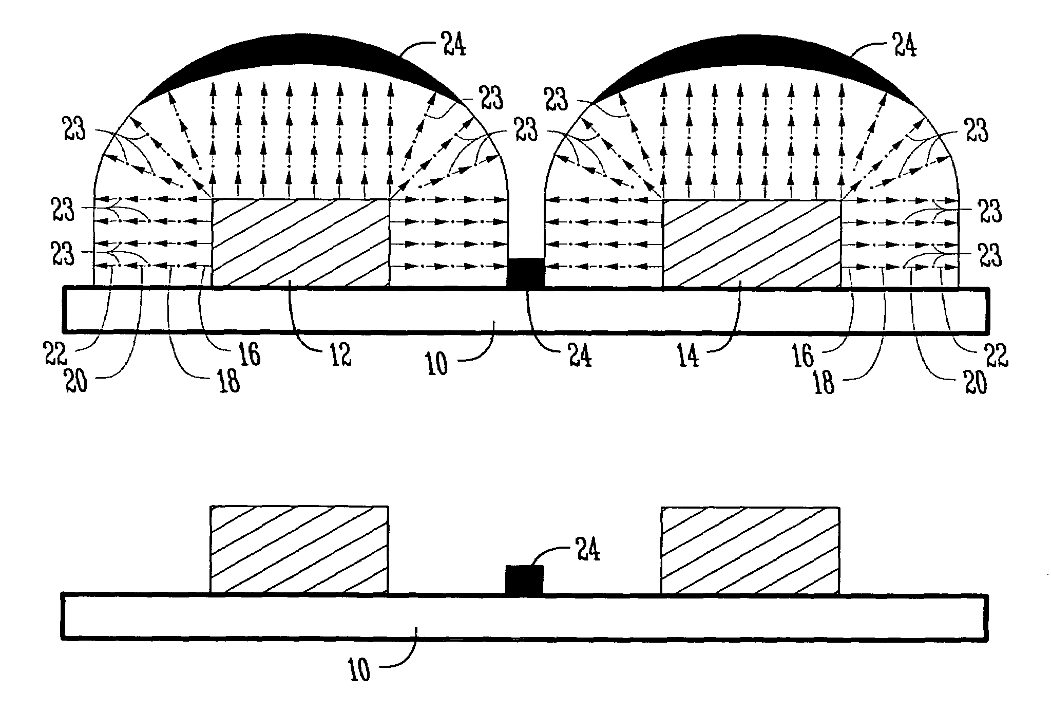
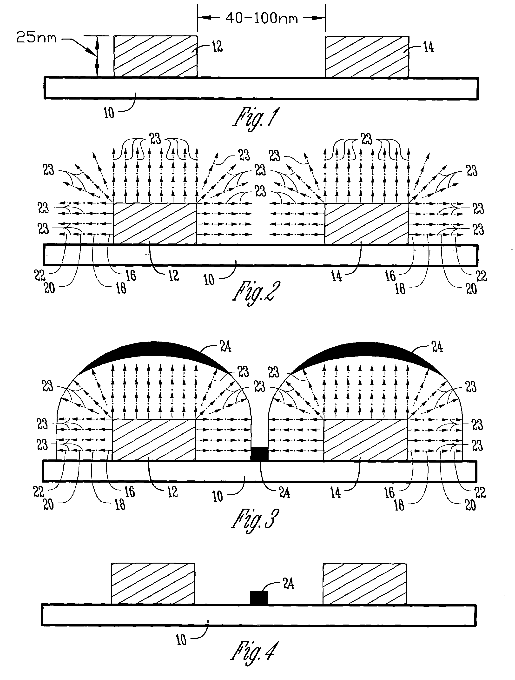
[0034]In FIG. 1, a substrate 10 is shown. The substrate may be a silicon substrate. Tests were conducted using a thermally oxidized highly polished doped Silicon substrate, Si(100). The present invention contemplates that other types of substrates may be used. The substrate is selected to ensure that essentially no multilayer resist adsorption occurs on the Si substrate.

[0035]A parent structure is deposited on the substrate. The parent structure of FIG. 1 includes trace 12 and trace...


PUM


Abstract

The present invention is a method and apparatus relating to manufacturing nanostructure patterns and components using molecular science. The method includes overlaying a multilayer organic molecule resist on at least a portion of a parent structure selectively deposited on a substrate, depositing a layer over the parent structure and in contact with at least a portion of the multilayer organic resist, and removing the multilayer organic molecule resist to leave a residual structure.

Description

CROSS-REFERENCE TO RELATED APPLICATIONS[0001]This application is a continuation of Provisional Application Ser. No. 60 / 209,377 filed Jun. 5, 2000, the disclosure of which is hereby specifically incorporated by reference.GRANT REFERENCE[0002]Work for this invention was funded in part by a grant from the United States Army Research Office, Army Research Office Grant No. DAAD 19-99-1-0269. Work for this invention was also funded in part by a grant from the Defense Advanced Research Projects Agency and the Office of Naval Research, DARPA / ONR Grant No. R13163-41600099, A04. Work for this invention was further funded in part by a grant from the National Science Foundation, Grant No. PHY-9983214. The government may have certain rights in this invention.FIELD OF THE INVENTION[0003]This invention relates generally to the field of nanofabrication. More specifically, the invention relates to methods of fabricating nanostructures using molecular multilayers and self assembly ruler. The inventio...

Claims


Application Information

Patent Timeline
Patent Type & Authority Patents(United States)
IPC IPC(8): H01L51/40
CPCB82B3/00B82Y30/00B82Y40/00Y10S977/89G03F7/40
Inventor WEISS, PAUL S.HATZOR, ANAT
Owner PENN STATE RES FOUND
Why Eureka
Try Eureka