
Method and apparatus for determining plasma impedance

a plasma and impedance technology, applied in the field of plasma processing, can solve the problems of inability to precisely install a voltage-current (“vi), inability to directly measure the rf impedance in the chamber, and inherently difficult to handle plasma, etc., and achieve the effect of accurate measurement of the rf impedan

Inactive Publication Date: 2006-03-21
TOKYO ELECTRON LTD
View PDF6 Cites 9 Cited by
  • Summary
  • Abstract
  • Description
  • Claims
  • Application Information

AI Technical Summary

Benefits of technology

Enables accurate and non-intrusive measurement of plasma RF impedance, reducing downtime and improving diagnostic capabilities for plasma processing, including real-time multi-frequency diagnostics and condition assessment of the processing chamber.

Problems solved by technology

However, plasma is an inherently difficult medium to handle, and direct measurement of plasma RF impedance in the chamber is nearly impossible, as it is very difficult to precisely install a voltage-current (“VI”) probe at a boundary between the plasma and a chamber wall.
Moreover, even if the probes can be made very small, and therefore, possible to install sufficiently near the interface, there still remain the mechanical and electrical problems of leading the RF signals out via wires, etc., through the insulator which needs to be vacuum tight.
When such deposition accumulates to a certain amount, it separates from the inner surfaces to become loose particles that can contaminate a wafer being processed.
However, the interior condition of a chamber is not readily apparent to a system operator, such that frequent disassembly and cleaning must be performed to ensure that the chamber is in a proper condition for plasma processing.
Because of this, a chamber may be dissembled and cleaned even when the amount of deposition has not accumulated to an amount detrimental to plasma processing, resulting in unnecessary downtime of the processing tool.
Moreover, when the chamber is disassembled and reassembled for preventive maintenance, no current method exists for ascertaining that the chamber exhibits the same RF characteristics as before disassembly and / or being contaminated by process.
A number of techniques have been developed to address the above-described concerns; however, such techniques have proven to be intrusive to the plasma process

Method used


Image

  • Method and apparatus for determining plasma impedance
  • Method and apparatus for determining plasma impedance
  • Method and apparatus for determining plasma impedance

Examples


Embodiment Construction

[0021]Referring now to the drawings, where like reference numeral designations identify the same or corresponding parts throughout the several views, several embodiments of the present invention are next described.

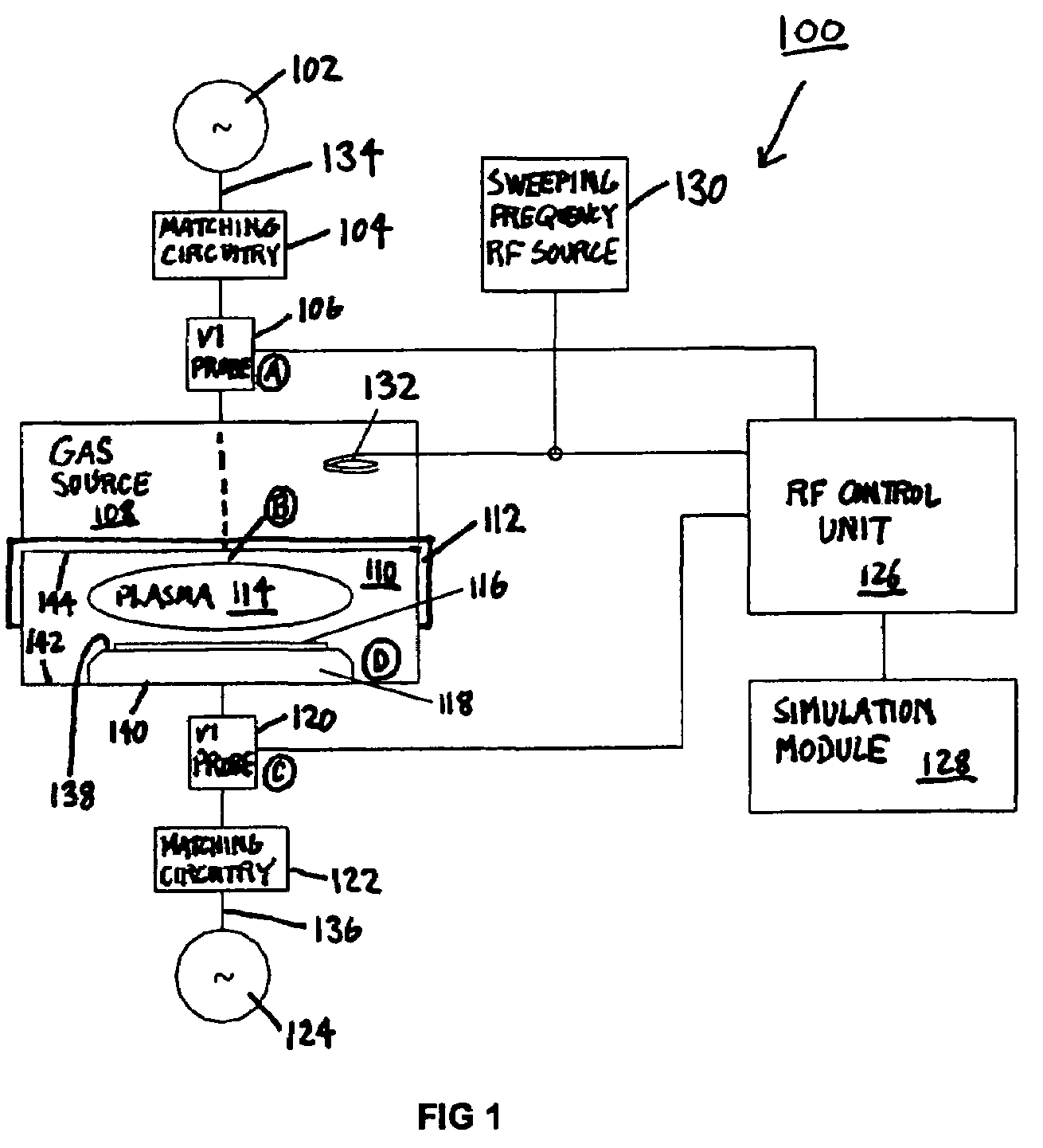
[0022]FIG. 1 illustrates a plasma processing system 100, which can be configured as an inductively coupled plasma (ICP) system, a capacitively coupled plasma (CCP) system, or a magnetically enhanced reactive ion etching (MERIE) system, for example. System 100 is primarily used to provide etching of a wafer 116 within chamber 110, where wafer 116 is supported by a support surface 138 of chuck 118. A bottom surface 140 of chuck 118 contacts an interior surface 142 of chamber 110. The etching, deposition, or other plasma processing of wafer 116 is performed using a plasma 114 created from gas provided by gas source 108.

[0023]Plasma 114 is driven by a main RF power source 102, which transmits RF power via an RF matching circuitry 104 to an excitation element 112. Excitation el...


PUM

PropertyMeasurementUnit
areaaaaaaaaaaa
voltageaaaaaaaaaa
radio-frequency impedanceaaaaaaaaaa

Abstract

A plasma processing system, method, and computer readable medium for measuring plasma impedance. The system includes a chamber configured to contain a plasma and including a chuck within an interior area of the chamber, the chuck including a support surface and a bottom surface, and a first voltage-current probe positioned at a first position located exterior to the chamber and on a radio-frequency transmission line between the chamber and a power source. The system also includes a simulation module connected to the first voltage-current probe and arranged to solve, based on measurements transmitted from the first voltage-current probe, a radio-frequency model of the radio-frequency transmission line between the first position and a second position located within the chamber.

Description

BACKGROUND OF THE INVENTION[0001]1. Field of the Invention[0002]The present invention is generally related to plasma processing and, more particularly, to a method and apparatus for determining plasma impedance using a modeled radio frequency transmission line.[0003]2. Discussion of the Background[0004]Plasmas are widely used in a variety of integrated circuit fabrication processes, including plasma etching and plasma deposition applications. Generally, plasmas are produced within a processing chamber by introducing a low-pressure process gas into the chamber and then directing electrical energy into the chamber for creating an electric field therein. The electric field creates an electron flow within the chamber that ionizes individual gas molecules by transferring kinetic energy to the molecules through individual electron-gas molecule collisions. The electrons are accelerated within the electric field, producing efficient ionization of the gas molecules, and the ionized particles...

Claims


Application Information

Patent Timeline
Patent Type & Authority Patents(United States)
IPC IPC(8): B23K10/00B23K9/00B23K9/02H01J37/32H01LH05H1/46
CPCH01J37/32082H05H1/46H01J37/32935H01J37/32174
Inventor MITROVIC, ANDREJ S.
Owner TOKYO ELECTRON LTD
Learn More