Protection of work piece during surface processing

a work piece and surface processing technology, applied in the direction of grinding drives, grinding machine components, manufacturing tools, etc., can solve the problems of higher failure rate of wafers, and cracking of wafers, so as to facilitate use, improve grinding and similar operations, and reduce wafer thickness

Inactive Publication Date: 2006-03-28
STRASBAUGH +1
View PDF135 Cites 15 Cited by
  • Summary
  • Abstract
  • Description
  • Claims
  • Application Information

AI Technical Summary

Benefits of technology

[0009]In some applications, a wafer substrate undergoes grinding to a desired thickness on the order of 25 to 150 microns, with desired wafer Total Thickness Variation (TTV) on the order of 3 microns or less. Such thinning processes are typically carried out in so-called “back grinding” or “backside grinding” operations where a wafer is placed face down with its front side (i.e., side at which devices are located) on a retention device while the exposed backside is ground, reducing the wafer thickness. The present apparatus and method additionally facilitates the use of special protective materials or tapes attached to the front surface of a wafer or work piece, which have desirable properties other than for back grinding protection. In this way these special tapes can be accommodated during back grinding since the method described herein provides back grinding protection.
[0010]It is one feature of the present invention, in some embodiments, to improve grinding and similar operations on work pieces held by hard chucks, particularly work pieces which are ground to relatively thin dimensions. It is another feature of the present invention, in some embodiments, to provide a backside grinding system that is capable of grinding a wafer to very thin dimensions without cracking the wafer. Another feature of the present invention, in some embodiments, is to provide wafer grinding techniques to reliably achieve wafer thickness of two hundred microns or less with attractive yield levels.
[0011]Yet a further feature of the present invention, in some embodiments, is to provide a front side wafer protection layer without using conventional adhesive backing tape applied to the wafer, thus eliminating issues surrounding backing tape, such as the risk of wafer breakage during tape removal, and reducing costs associated with the tape.
[0012]A further feature of the present invention, in some embodiments, is to provide wafer grinding techniques that do not require a side, e.g., a front side, of the wafer to be protected by a tape, a photo resist layer or other covering.
[0013]Another further feature of the present invention, in some embodiments, is to provide a protection / securing layer for distributing vacuum forces on the front side of a wafer. Another feature of the present invention, in some embodiments, is to provide wafer grinding techniques in which taping and de-taping of the front side surface (circuitry side) of the wafer is eliminated. An additional feature of the present invention, in some embodiments, is to provide a reusable protecting / securing protective layer. These and other features, advantages and benefits of the present invention are attained, in accordance with one embodiment, in an arrangement for supporting a wafer having opposed first and second major surfaces, during grinding of the first surface, without using protective tape to protect the second surface, including a chuck including a chuck body and a support surface; and a protective material, held fixed in relation to the support surface, wherein the second surface of the work piece is selectively held in relation to the support surface, with the protective material being interposed therein between, whereby the second surface of the work piece is protected by the protective material during grinding of the first surface.

Problems solved by technology

Problematically, the taping and de-taping process results in cracking of the wafer in some cases, especially for wafers thinned below a 200 μm thickness.
These cracks can be due to localized forces that are created between the tape and the wafer, or as a result of forces exerted when the tape is pulled from the front side of the wafer against the adhesive.
As a result, a higher rate of failure is seen when wafers are taped and de-taped.
Because of the additional steps of taping and de-taping, and of the relatively higher rate of failure of the wafer resulting from the taping and de-taping process, taping and de-taping results in a relatively decreased wafer processing throughput.
Further, because de-taping subjects the wafer to mechanical stresses, and thus limits the thinness of the wafer due to the need to maintain at least some minimum degree of mechanical integrity sufficient to withstand the forces applied during de-taping, minimum wafer thinness has heretofore been limited to 150 to 200 microns.
Further disadvantageously, the taping and de-taping processes add cost due to equipment, and require valuable floor space for taping and de-taping equipment.

Method used


Image

  • Protection of work piece during surface processing
  • Protection of work piece during surface processing
  • Protection of work piece during surface processing

Examples


Embodiment Construction

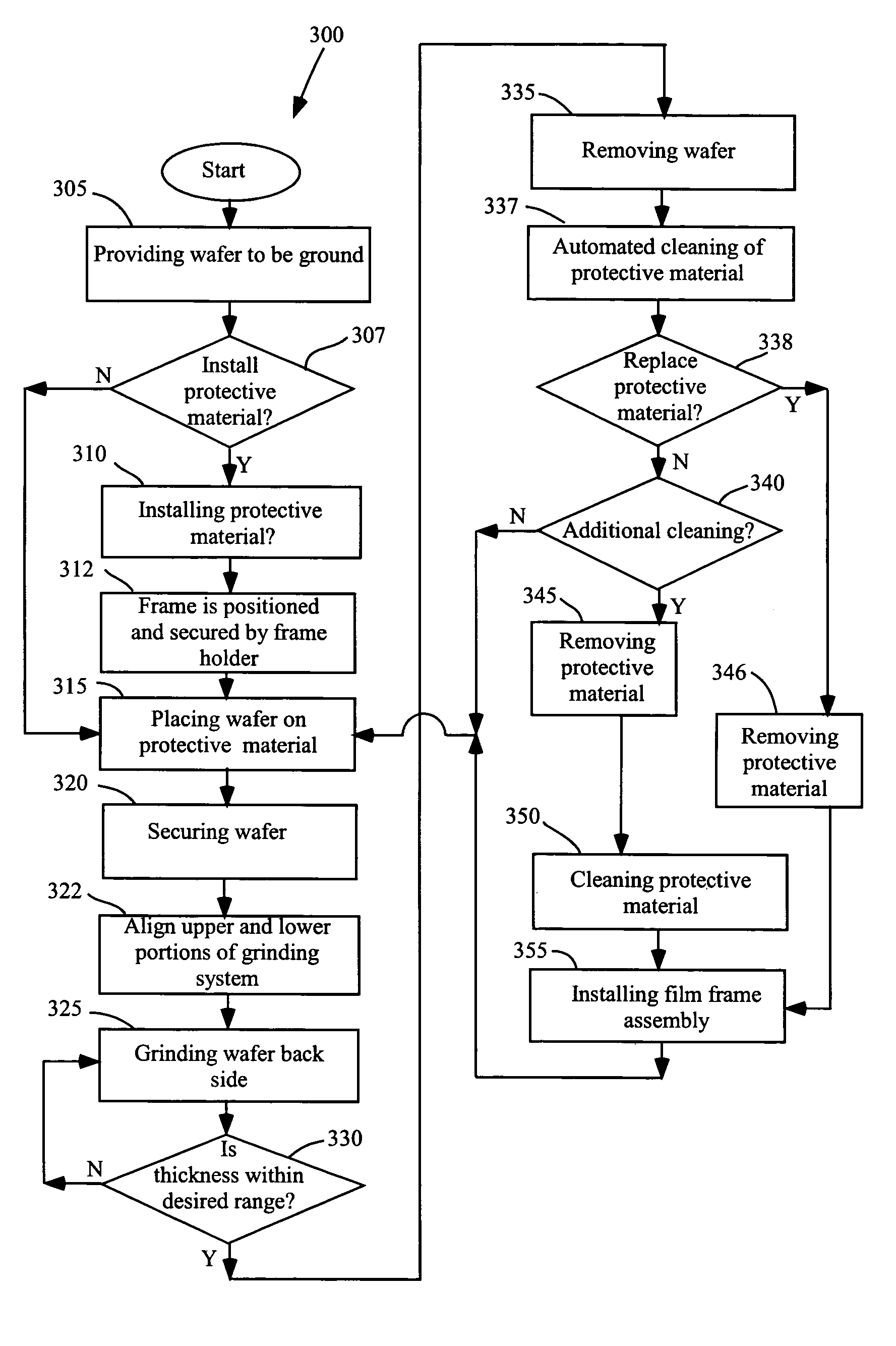
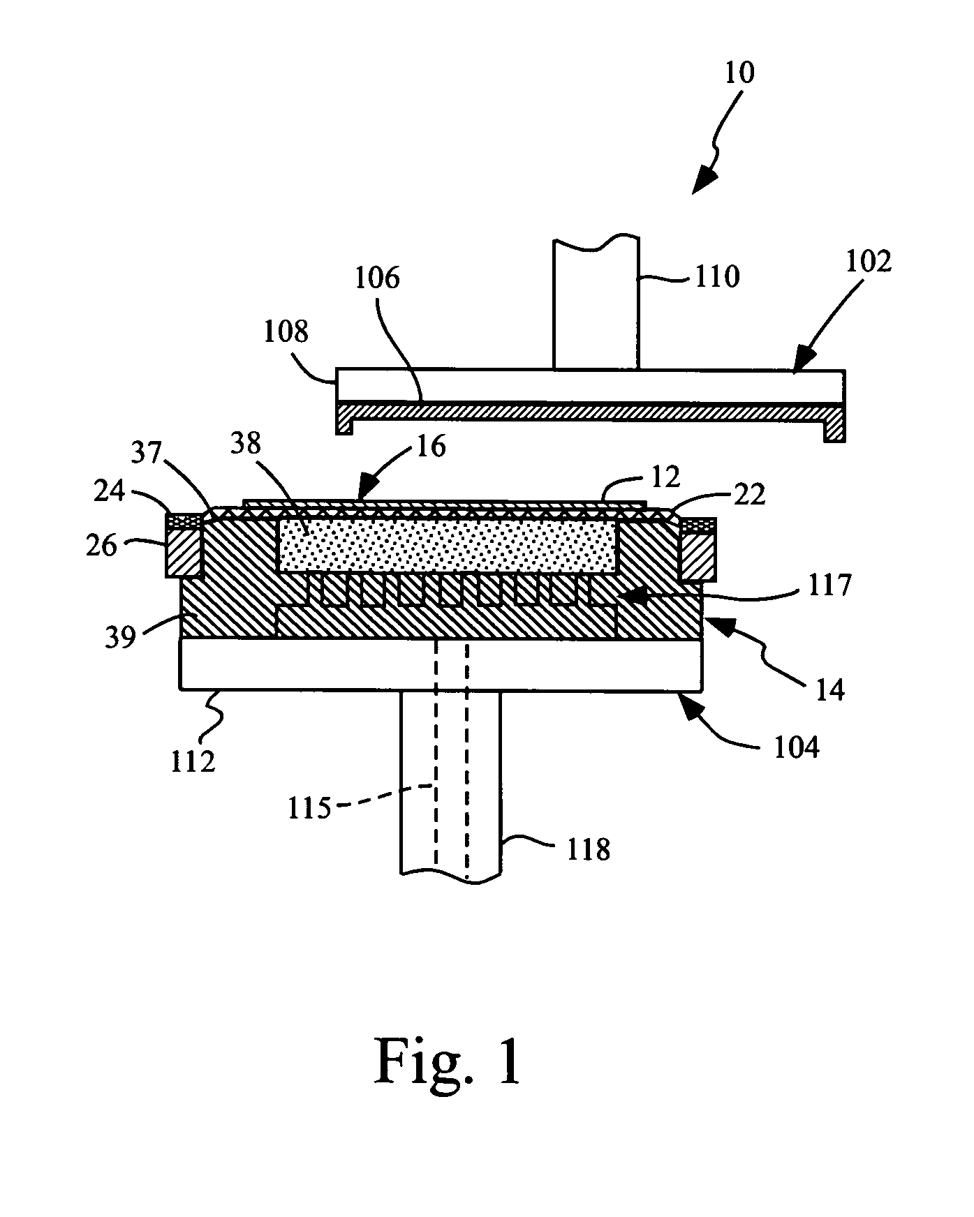
[0021]As will be seen herein, the present embodiment offers substantial improvements in the field of semiconductor grinding or polishing on either the front or backside of a wafer being processed. The present embodiment has found immediate commercial application in the field of wafer thinning, which is typically carried out on the backside of the wafer. The present embodiment provides a number of important advantages by at least in part eliminating the need for taping and de-taping procedures, including increased production speeds, increased end product throughput, reduced costs, as well as other advantages and enhancements.

[0022]In previous grinding systems, wafer taping procedures utilizing protective tape can achieve minimum wafer thicknesses down to about 180 microns with a total thickness variation (TTV) of 4 to 5 microns. The present embodiment also eliminates the need for coating a front wafer surface with a spun photo resist. With the present embodiment, minimum wafer thickn...


PUM

PropertyMeasurementUnit
thicknessaaaaaaaaaa
Thicknessaaaaaaaaaa
Thicknessaaaaaaaaaa

Abstract

The present invention provides an apparatus and method for protecting a work piece during surface processing. The apparatus employs a protective material to protect a wafer during backside grinding. The apparatus can further include a vacuum chuck that allows the passage of a vacuum signal, a frame holding the protective material, a frame holder to hold the frame, and a fastening arrangement to fasten the frame holder to the chuck adjacent a support surface. The method provided by the invention can include providing a vacuum chuck, placing a protective material in contact with the chuck, placing a wafer in contact with the protective material, applying a vacuum signal securing the wafer with the chuck, and grinding the backside surface of the wafer.

Description

CROSS REFERENCE TO RELATED APPLICATIONS[0001]This application claims priority under 35 U.S.C. § 119(e) to U.S. Provisional Patent Application No. 60 / 371,388, filed Apr. 9, 2002, of Salman Moudrek Kassir and Larry A. Spiegel, for IMPROVED BACKSIDE PREPARATION OF SEMICONDUCTOR WAFERS, which U.S. Provisional Patent Application is hereby fully incorporated herein by reference.BACKGROUND OF INVENTION[0002]The present invention pertains to the support of work pieces such as semiconductor wafers, and in particular to support of work pieces during grinding or polishing. Presently, conventional semiconductor wafers on which circuit patterns are formed on one side (a front side) are subjected to a grinding process so as to reduce the overall thickness of the wafer. Grinding is performed on the back surface of the wafer where there is no circuitry pattern. The resultant thinning of the wafer allows for the production of thinner packaged electronic chips, microchips, and the like. Additionally,...

Claims


Application Information

Patent Timeline
Patent Type & Authority Patents(United States)
IPC IPC(8): B24B49/00B24B1/00B23B31/30B24B37/30H01L21/304H01L21/683
CPCB23B31/307H01L21/6838B24B37/30B23B2226/18
Inventor KASSIR, SALMAN MOUDREKSPIEGEL, LARRY A.
Owner STRASBAUGH
Why Eureka
Try Eureka