Multi-band low noise amplifier system

a low-noise amplifier and multi-band technology, applied in the direction of low-noise amplifiers, amplifier combinations, amplifier modifications to reduce noise influence, etc., can solve the problems of increasing the cost per square millimeter of silicon, and significantly worsening the quality of metal interconnects, etc., to achieve less silicon area, eliminate additional insertion loss and noise figure, and increase/decrease the effective inductance

Active Publication Date: 2006-04-04
TEXAS INSTR INC
View PDF4 Cites 150 Cited by
  • Summary
  • Abstract
  • Description
  • Claims
  • Application Information

AI Technical Summary

Benefits of technology

[0007]The present invention is directed to a system and method for implementing a low noise amplifier (LNA) that operates over multiple frequency bands while occupying less silicon area than known LNA implementations. The LNA includes output matching that can be tuned by an adjustable inductor together with a tunable capacitor bank. The adjustable inductor can be implemented in various ways such by using the technique disclosed by Seong-Mo Yim and Kenneth, K. O., “Demonstration of a switched resonator concept in a dual-band monolithic CMOS LC-tuned VCO,”IEEE Conference of Custom Integrated Circuits, pp. 205–208, May 2001, of using a switch to short a section of the inductor metal winding, or by using a magnetic coupling to increase / decrease the effective inductance, or by using a combination of the two approaches. The LNA topology can be easily extended to a differential LNA and requires no external switches, thus eliminating the additional insertion loss and noise figure. The LNA topology further preserves the filtering / rejection to interferers associated with more conventional LNAs, relaxing LNA linearity requirements. Superior isolation is achieved between multiple input signals while allowing use of antenna filters available in the market to reduce overall cost. All desired frequency bands are accommodated on the PCB during the ON state.
[0009]a plurality of DC biasing circuits, each DC biasing circuit operational to provide a DC bias source for a single RF input stage and to increase isolation from other input stages;

Problems solved by technology

Such traditional approaches are disadvantageous in that 1) a huge semiconductor area is required by multiple LNAs and mixers, and 2) long interconnect routings over a large area are needed but maintaining a low signal loss, low parasitic resistance and low parasitic capacitance for such routings is very difficult to achieve.
As CMOS technology continues to scale down, the silicon cost per square millimeter (mm2) increases dramatically; and the metal interconnect quality becomes significantly worse such that metal routing across a large area becomes a major concern.
The foregoing techniques are disadvantageous in that 1) they need external switches to select between different matching networks, thus increasing insertion loss and noise figure (NF); 2) they have inferior filtering / rejection to interferers due to either broadband matching or multiple resonant frequencies of the matching networks, thus increasing the LNA linearity requirement; 3) they have inferior isolation between multiple input signals because there is only one input node to the LAN, particularly if the frequencies of the multiple radio standards are not distant; 4) there is not an antenna filter available in the present market to support multiple frequency bands; and 5) although for systems such as GPRS and EDGE, there is only one frequency band that needs to be active at any time on the IC, the filters on the PCB cannot be turned off, resulting in large interference from the inactive to the active frequency bands.

Method used


Image

  • Multi-band low noise amplifier system
  • Multi-band low noise amplifier system
  • Multi-band low noise amplifier system

Examples


Embodiment Construction

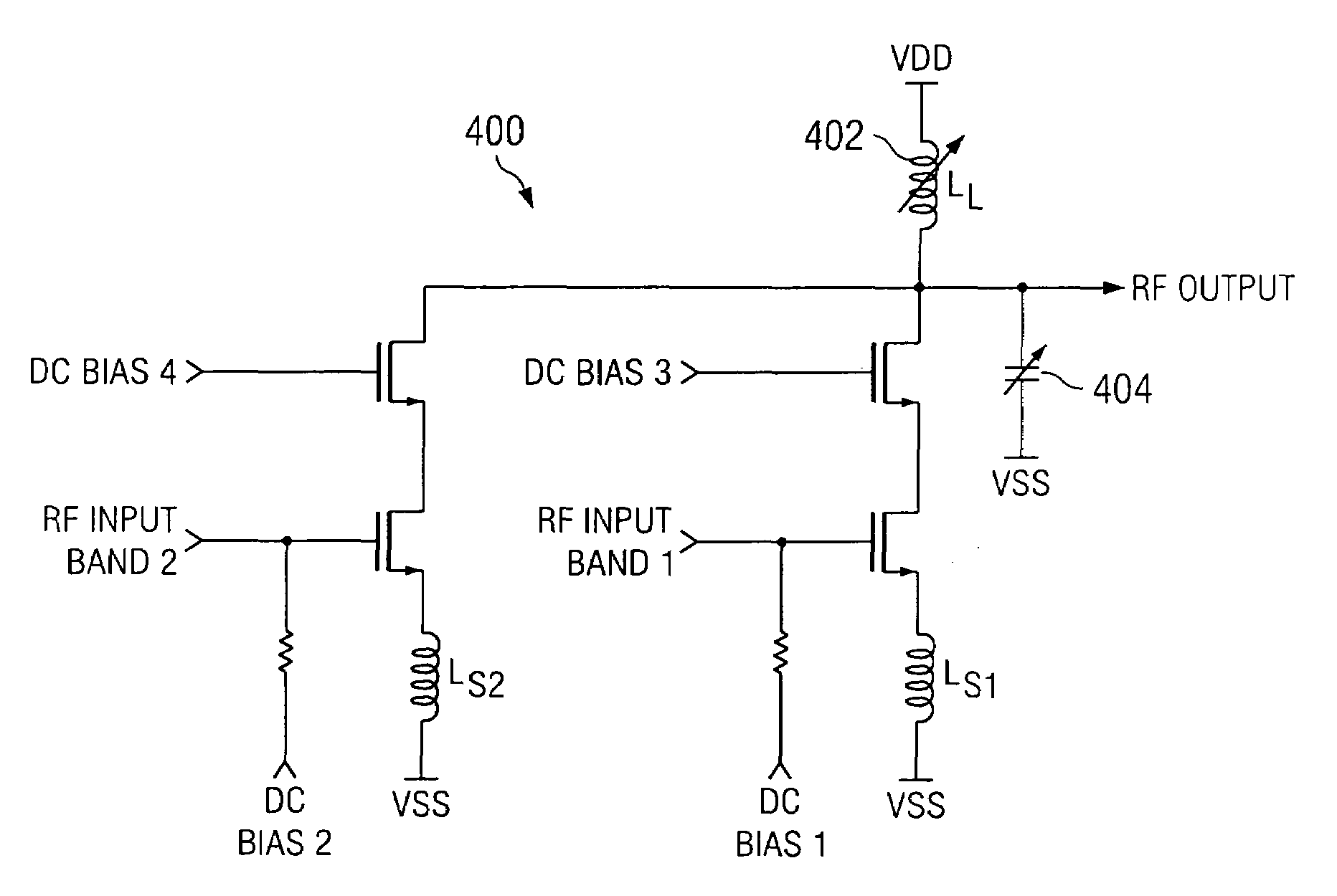
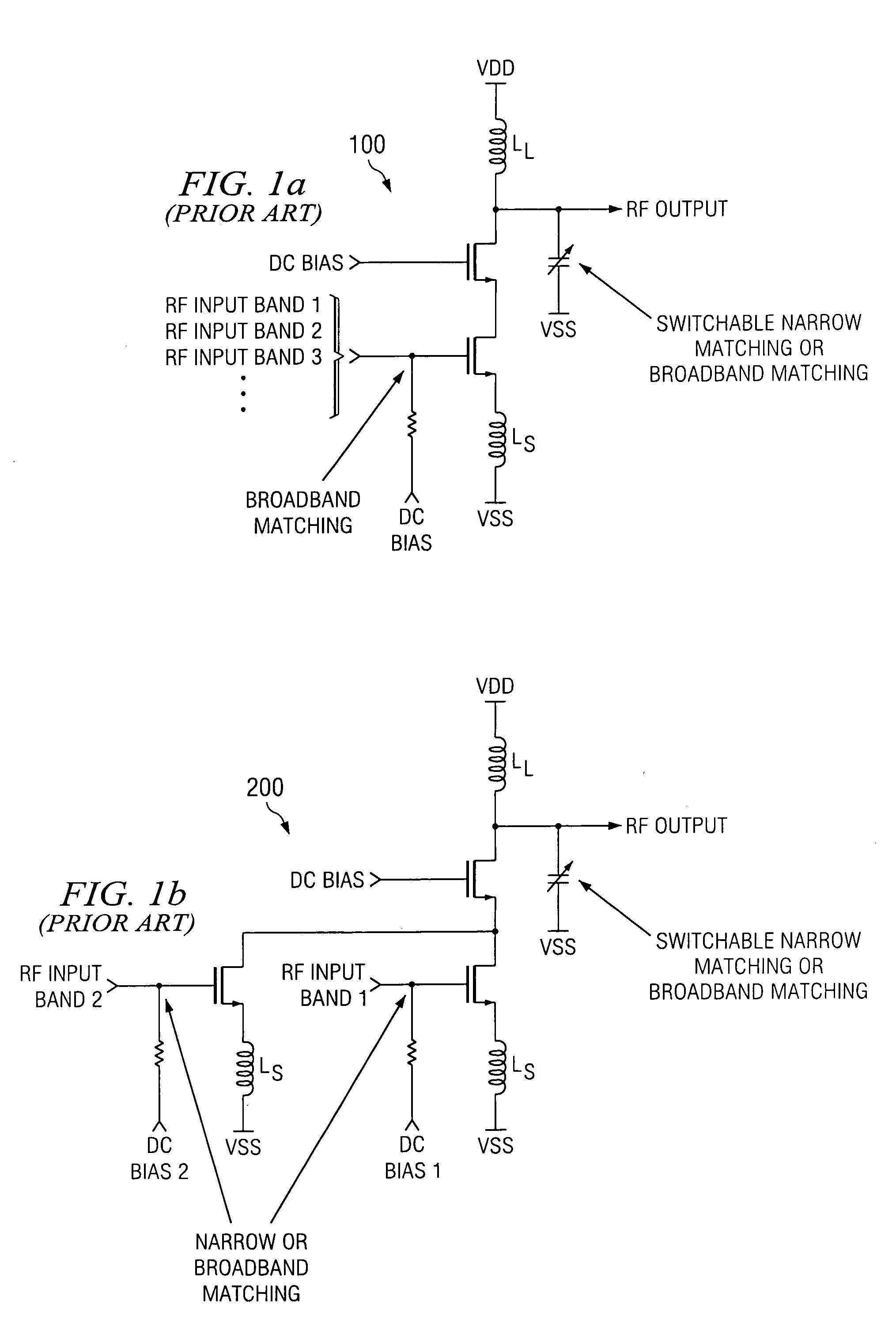
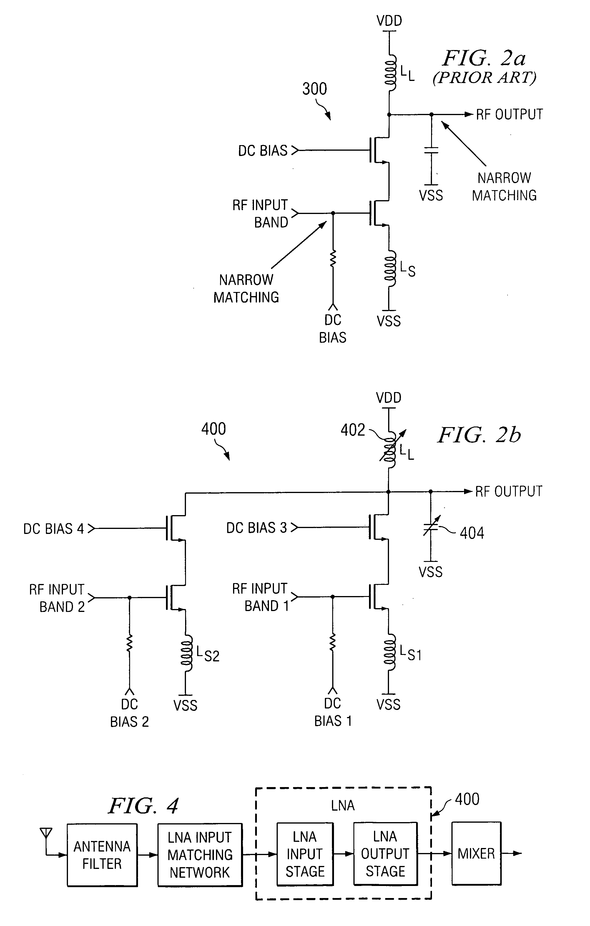
[0036]FIG. 2(a) illustrates a typical prior art single (narrow)-band LNA 300, while FIG. 2(b) illustrates a multi-band LNA circuit topology 400 according to one embodiment of the present invention. The circuit topology 400 can be easily extended to a differential LNA that will be discussed herein below in further detail following a detailed discussion of the circuit topology 400. FIG. 4 is a block diagram illustrating the signal flow through the LNA 400 depicted in FIG. 2(b), and is provided to enhance clarity and understanding of the embodiments described herein below.

[0037]The single (narrow)-band LNA 300 typically is employed on a PCB having separate antenna filters providing individual outputs for each frequency band. An individual input bondpad thus receives only one signal from one filter, which is then amplified without interfering with other signals. The source degeneration inductors, Lsn, where n is an integer, seen in FIG. 2(b) can be reduced to 1, depending upon the circu...


PUM


Abstract

A low noise amplifier (LNA) operates over multiple frequency bands while occupying less silicon area than known LNA implementations. The LNA includes output matching that can be tuned by an adjustable inductor together with a tunable capacitor bank.

Description

BACKGROUND OF THE INVENTION[0001]1. Field of the Invention[0002]This invention relates generally to integrated circuits, and more particularly to a system and method for implementing a low noise amplifier (LNA) that operates over multiple frequency bands while occupying less silicon area than known LNA implementations.[0003]2. Description of the Prior Art[0004]Single integrated circuit chips required to support multiple radio standards one at a time have typically done so with multiple circuit blocks / modules in the IC in which each block / module has accommodated only a single radio standard. Enhanced Data Rates for GSM (EDGE) and General Packet Radio Services (GPRS) have traditionally been designed using three or four Low-Noise Amplifiers (LNAs) cascading with the same number of mixers in which the outputs are merged together feeding a single IF / baseband circuit. Such traditional approaches are disadvantageous in that 1) a huge semiconductor area is required by multiple LNAs and mixe...

Claims


Application Information

Patent Timeline
Patent Type & Authority Patents(United States)
IPC IPC(8): H03F3/68H03F1/22H03F3/191H03F3/193
CPCH03F1/223H03F3/193H03F3/45179H03F1/565H03F2200/294H03F2200/492H03F2203/45394H03F2203/7209H03F2200/372H03F1/22H03F1/26H03F3/191
Inventor HUNG, CHIH-MINGLEIPOLD, DIRKHO, YO-CHUOL
Owner TEXAS INSTR INC
Why Eureka
Try Eureka