Multiplexed-input-separated sigma-delta analog-to-digital converter design for pixel-level analog-to-digital conversion

a digital converter and multi-input technology, applied in the field of pixel-level analog-to-digital conversion, can solve the problems of high power consumption, small format and/or high price of ccd imagers, and fabrication technology that requires dedicated and costly manufacturing processes, etc., and achieves low power consumption, high linearity, and low cost

Inactive Publication Date: 2006-04-04
UNIVERSITY OF ROCHESTER
View PDF14 Cites 47 Cited by
  • Summary
  • Abstract
  • Description
  • Claims
  • Application Information

AI Technical Summary

Benefits of technology

[0029]It is an object of the invention to combine the small pixel size offered by performing analog-to-digital conversion away from the pixel level with the advantages in terms of high linearity, low power consumption and the like offered by performing analog-to-digital conversion at each pixel. To achieve the above and other ends, the present invention uses a multiplexed-input-separated ΣΔ ADC at each row rather than at each pixel. In one embodiment, an input transistor of the integrator and an external capacitor are supplied at the pixel level; while the remainder of the integrator and entire quantizer are supplied at the row level. In another embodiment, in which the photodetecting element is used as an integrator, the input transistor of the quantizer is supplied at the pixel level, while the remainder of the quantizer is supplied at the row level.
[0031]The present invention uses a Multiplexed-Input-Separated Sigma-delta ADC, which provides a dynamic range much improved over the Nyquist ADC architecture. This image sensor with a pixel-level ADC embodies the advantages of both modern over-sampling sigma-delta ADC's and the design principles of low transistor count CMOS imager pixel readout circuits. Due to the over-sampling nature of the architecture, the transistors can be small to enable high resolution with a high fill-factor. The design inherently has high linearity and low power consumption. The dynamic range of the design is intrinsically greater than 78 dB, or 13 bits, but could be greater by running at higher sampling frequency and higher power drain.
[0032]The present claimed invention offers the following advantages over the technology of the Mandl patents. In embodiments with external capacitance, the integrator can be supplied at the row level rather than the pixel level, thus decreasing minimum pixel size and increasing fill factor. In embodiments in which the photodetector is used as an integrator, the input transistor is supplied at the pixel level, thus reducing crosstalk. All embodiments can be implemented using standard technologies such as CMOS.

Problems solved by technology

However, the biggest disadvantage of CCD imagers is their small format and / or high price.
CCD sensors also rely on specialized fabrication technology that requires dedicated and costly manufacturing processes.
The drawbacks of CCD imaging technology are the following:
High-power consumption,
Random pixel access is not possible, i.e., pixels must be read out sequentially making it impossible for CCD imagers to easily access a subset of pixels within an image,
Due to losses there is a maximum safe shifting distance limiting the practical size of the image sensor
Relatively slow frame rates
For example, CMOS image sensors can be made at standard manufacturing facilities that produce almost 90% of all semiconductor chips, which significantly decreases their designing and manufacturing costs.

Method used


Image

  • Multiplexed-input-separated sigma-delta analog-to-digital converter design for pixel-level analog-to-digital conversion
  • Multiplexed-input-separated sigma-delta analog-to-digital converter design for pixel-level analog-to-digital conversion
  • Multiplexed-input-separated sigma-delta analog-to-digital converter design for pixel-level analog-to-digital conversion

Examples


Embodiment Construction

[0047]Preferred embodiments of the invention will be set forth in detail below with reference to the drawings, in which like reference numerals correspond to like elements throughout.

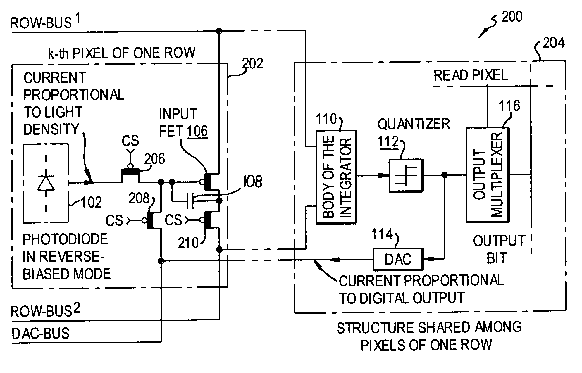
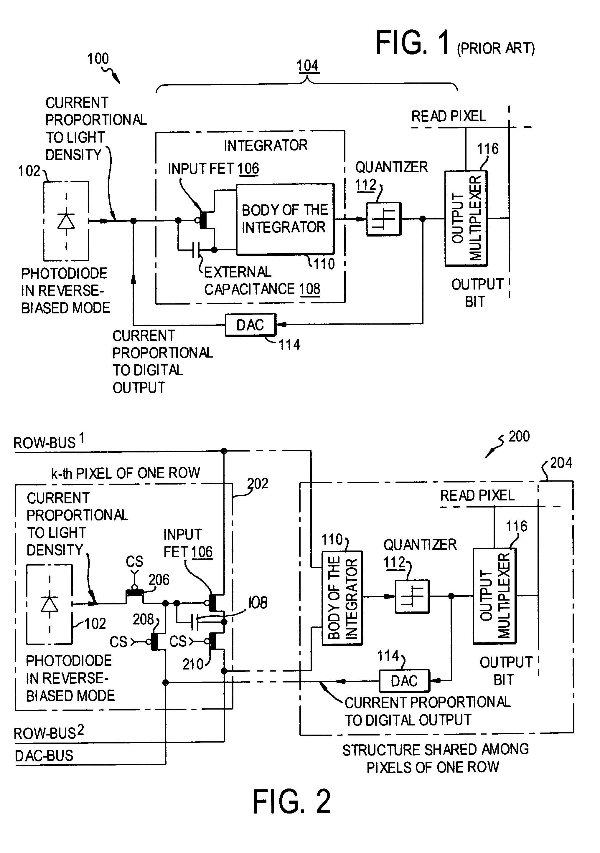
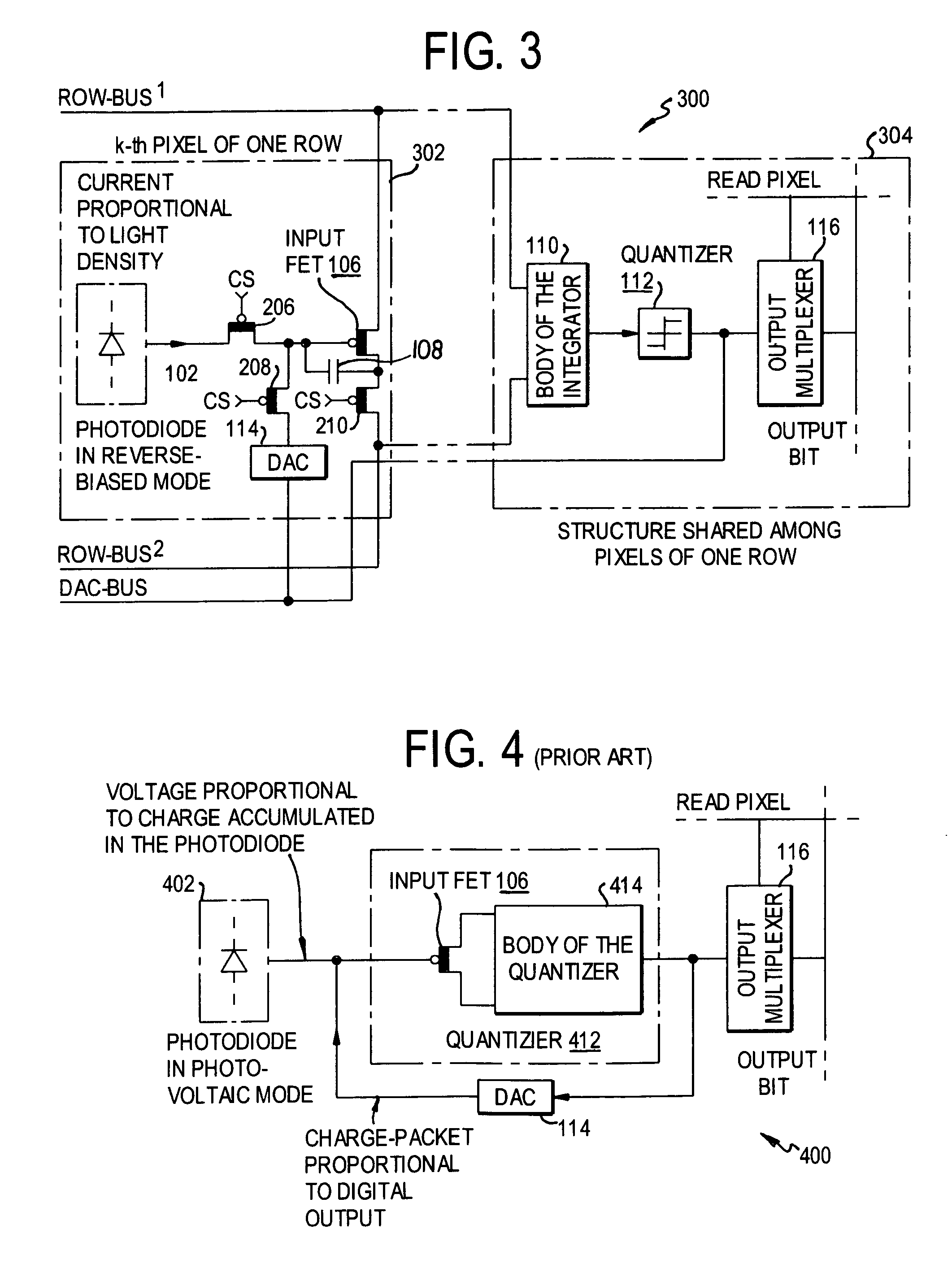
[0048]Each preferred embodiment uses one of two basic principles, one in which the intra-pixel integrator structure is realized with an external capacitance, and the other in which the integration effect of the photodiode in the photo-voltaic mode is used.

[0049]The first basic principle will be explained with reference to a block schematic of a known first-order pixel level ΣΔ ADC structure, where the intra-pixel integrator structure is realized with the external capacitance, as shown in FIG. 1. In the structure 100, a block 102 that represents a photosensitive element contains the photodiode and possibly a biasing circuit to keep the diode in the reverse-biased mode. While in reverse-bias mode, the voltage across the diode's terminals is kept constant, and the current is proportional to the light inten...


PUM


Abstract

An image-sensing element has an array of photodiodes or other photodetecting elements and performs sigma-delta analog-to-digital conversion on the outputs of the photodetecting elements. The sigma-delta analog-to-digital converters have components divided between pixel-level and row-level structures, with each row-level structure connected to its pixel-level structures to define a multiplexed-input-separated sigma-delta analog-to-digital converter. The converter can include an integrator or can rely on an integration effect of the photodetecting element. The feedback required for sigma-delta analog-to-digital conversion can involve digital-to-analog converters located at each row-level structure or at each pixel-level structure.

Description

REFERENCE TO RELATED APPLICATION[0001]The present application claims the benefit of U.S. Provisional Patent Application No. 60 / 486,468, filed Jul. 14, 2003, whose disclosure is hereby incorporated by reference in its entirety into the present disclosure.FIELD OF THE INVENTION[0002]The present invention is directed to a sigma-delta (ΣΔ) analog-to-digital converter (ADC) design and more particularly to a multipexed-input-separated (MIS) ΣΔ ADC design adapted for use as a pixel-level ADC in a pixel readout circuit employed in a CMOS image sensor.DESCRIPTION OF RELATED ART[0003]Charge-coupled-device (CCD) imagers were first developed in the 1970's in the defense sector but quickly found acceptance among professional astronomers when they began using CCD cameras instead of photographic films and plates. There were several advantages that favored CCD cameras over photographic film:[0004]CCD cameras are up to 100 times more sensitive than film[0005]CCD images are readily digitized, elimina...

Claims


Application Information

Patent Timeline
Patent Type & Authority Patents(United States)
IPC IPC(8): H03M3/00H01L27/00H03M1/12H03M3/02H04BH04N5/335
CPCH04N5/23241H04N5/335H03M3/474H03M3/456H03M3/43H04N25/00H03M3/00H03M1/12
Inventor BOCKO, MARK F.IGNJATOVIC, ZELJKO
Owner UNIVERSITY OF ROCHESTER
Why Eureka
Try Eureka