Method and apparatus for cutting ultra thin silicon wafers

a technology of silicon wafers and cutting methods, applied in metal sawing apparatus, metal sawing devices, manufacturing tools, etc., can solve the problems of undetectable high wire speed, damage and cracks in the wires, and more fragile diamond saw wires, so as to reduce the variation of total thickness, improve control and stabilization, and thin the effect of thin wafers

Inactive Publication Date: 2006-04-11
SOLAICX
View PDF12 Cites 43 Cited by
  • Summary
  • Abstract
  • Description
  • Claims
  • Application Information

AI Technical Summary

Benefits of technology

[0017]In order to overcome the foregoing limitations and disadvantages inherent in a conventional wire saw process for cutting silicon, an aspect of the invention provides a stabilizing strip system for holding the wafers invariantly against vibration during the sawing process. The stabilizing strip is applied to the ends of the partially defined wafers at an early stage in the sawing process when the wafers have been partially cut through a silicon ingot or block of silicon material. The stabilizing strip can be held in place by any convenient positioning means, such as adhesive material. The stabilizing strip serves to keep the silicon slices (the incipient wafers) separate, and prevents the slices from vibrating, oscillating, or touching during the slicing process.
[0018]The stabilizing strip system when combined with a conventional wire saw advantageously produces thinner, lightweight wafers with improved control and stabilization. Wafers produced by the stabilizing strip system are characterized by a minimized total thickness variation (TTV), substantially uniform planarity, and substantial elimination of bow and warp.
[0019]The stabilizing strip system also improves and accelerates handling of the wafers after the slicing is completed, further facilitates the cleaning process, and allows for more rapid or automated placement of the wafers in cassettes.
[0020]In accordance with another aspect of the invention, a wire saw system, comprising a stabilizing strip, uses a small diameter diamond coated or diamond impregnated wire and a very low viscosity fluid composition for cutting ultra thin silicon wafers. The diamond-coated or impregnated wire, being a fixed abrasive, can be operated at a much lower wire speed than in a conventional process. The lower wire speed in combination with the stabilizing strip for holding the wafers invariantly against vibration results in greatly reduced stress and lower hydraulic forces being imposed on the wafers. The stabilizing feature advantageously provides a dampening effect on vibration, thereby greatly reducing or substantially eliminating process stress within the wafers. This advantageously results in a structurally stronger wafer. Since lower wire speed reduces stress, this advantageously enables the use of smaller wires without breakage and further creates lower kerf loss and higher material utilization. This aspect of the invention further facilitates the slicing of ultra thin silicon wafers in a mass production process at reasonable cost.
[0021]The use of diamond impregnated wire also advantageously provides a fixed rate of abrasive particles thereby eliminating complex systems for varying the feed rate of slurry to compensate for variations in the rate of transport of abrasive grains, in contrast to a conventional wire saw system.
[0022]These and other features and aspects of the invention provide a process and apparatus for slicing very thin silicon wafers, down to dimensions on the order of 200 microns or less with superior physical properties, such as substantially uniform planarity, substantial elimination of bow or warp, low kerf loss, improved material utilization, and thus markedly lower cost than is currently possible using a conventional wire saw system.

Problems solved by technology

However, due to their smaller core diameter, diamond saw wires are more fragile.
Such mechanical sensitivity promotes damage and cracks in the wires at tensioning and guide rollers.
Since this is a free abrasive process, undesirably high wire speeds are required.
Also, large quantities of slurry are required for slicing and cooling.
Because of this, strong hydraulic forces are applied to the wafers being cut creating problems when slicing thin wafers.
Since a great amount of process stress is applied to the wafers, there is a further problem in that residual process distortion becomes great.
However, such conventional suspensions are not stable and do not provide uniform coating on the cutting wires.
Furthermore, such compositions require vigorous agitation to maintain uniform suspension of the particles, and the suspension settles out quickly under stagnant conditions, and even during workpiece slicing while still under agitation.
When cutting is done using conventional adhering free abrasive particles, or diamond wire, an extreme amount of process stress is applied to the wafers.
The force of the wires against the workpiece can deform the workpiece and degrade planarity characteristics in the resulting wafer, thus adding to the need for further processing time and adding to overall cost.
It also has been found that a conventional free abrasive wire or diamond-coated wire sawing process tends to cause the wafers to oscillate and to deform during the sawing process.
When slicing very thin wafers, one of the problems encountered is that as the wires progress downward through the ingot, unsupported sections of the wafers tend to vibrate, move, or stick together.
This disadvantageously imposes a limit on the thickness of wafers that can be achieved through a current mass production wire saw process.
Vibration and oscillation of the wafers also contribute to surface damage of the wafer such as wire marks that are difficult to remove and adversely affect wafer performance.
Conventional wire saws have disadvantages in attempting to provide a cost effective way to cut silicon into very thin wafers, with thicknesses down to 200 microns or less, that would be suitable for use in solar cells.
Imperfections due to process distortion or defects in planarity, warp, bow, variations in thickness and surface damage are still too prevalent to achieve cost effective mass production of ultra thin silicon wafers suitable as a starting base for a high efficiency low cost solar cell.

Method used


Image

  • Method and apparatus for cutting ultra thin silicon wafers
  • Method and apparatus for cutting ultra thin silicon wafers
  • Method and apparatus for cutting ultra thin silicon wafers

Examples


Embodiment Construction

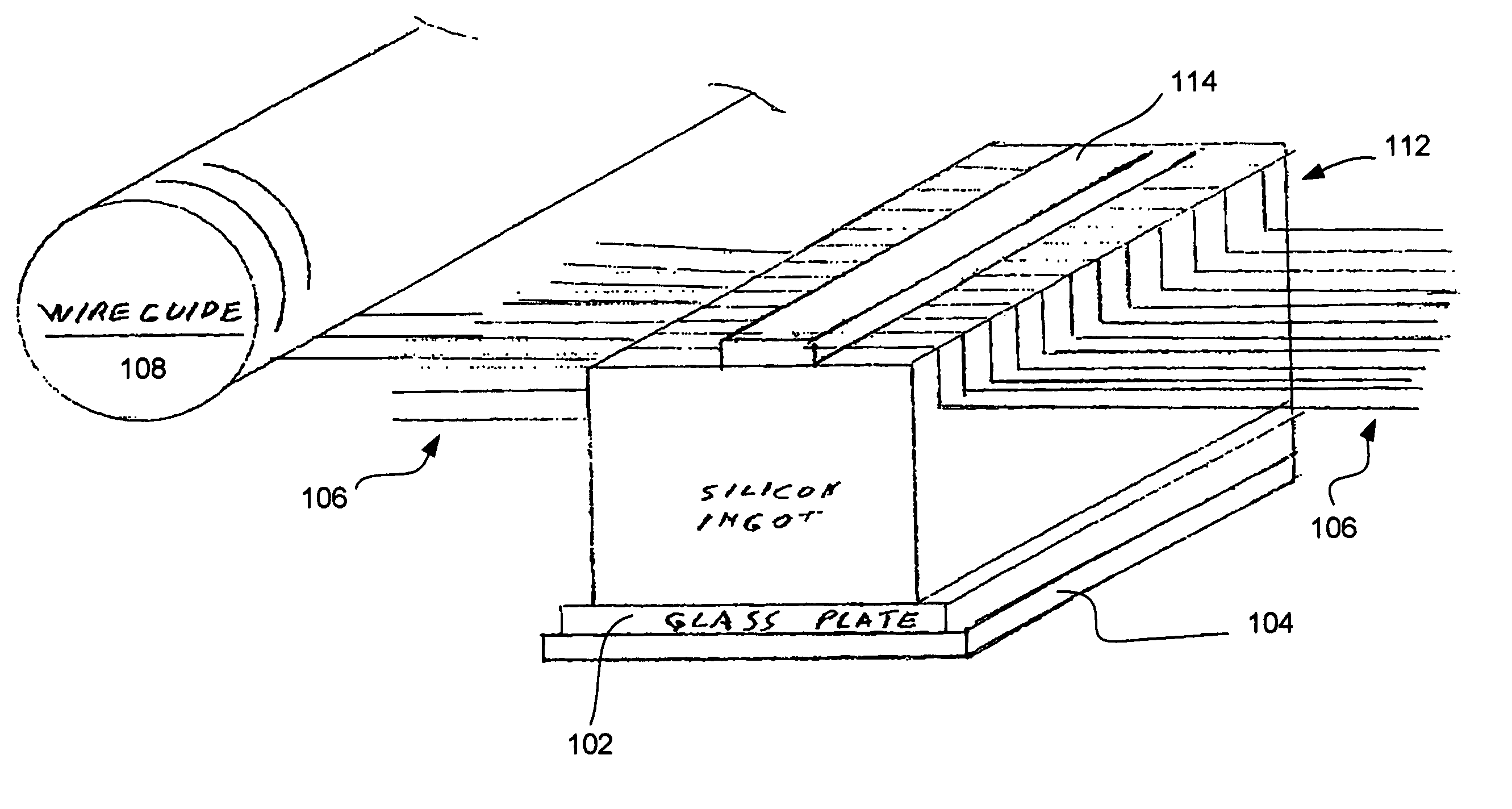
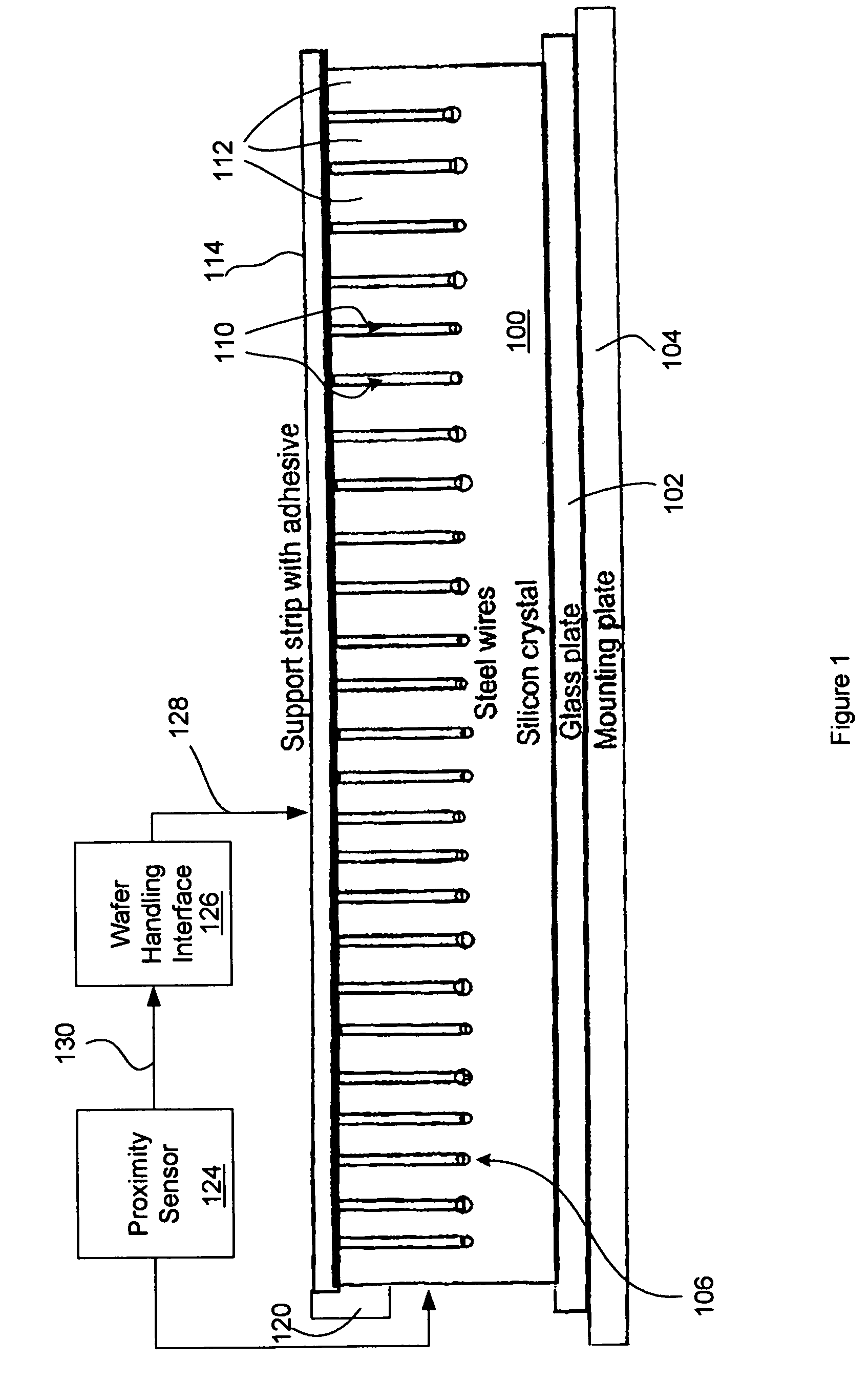
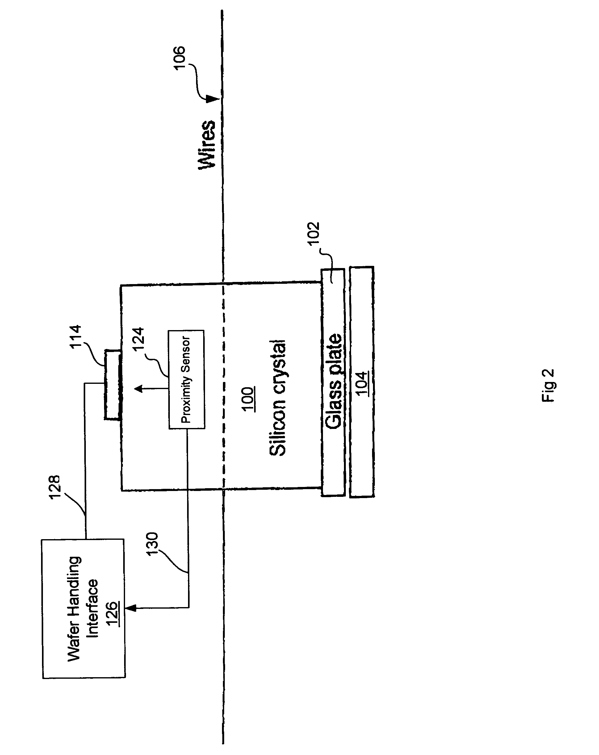
[0029]Referring to FIGS. 1, 2 and 3, an ingot or block of silicon 100 is provided on a glass plate or cutting beam 102. The cutting beam 102 also can be graphite epoxy or similar material, which in turn is positioned on a conventional mounting plate 104 for holding the block of silicon during the wire sawing process. The mounting plate slides into a fixture in the wire saw (not shown for clarity). The wire 106 is looped over the wire guide 108 (FIG. 3) to form a wire web comprising the plurality of cutting surfaces, each wire 106 providing a corresponding cut or section 110 through the silicon block 100. When cut all the way through to the cutting beam 102, the sections 110 define a plurality of ultra thin silicon wafers 112.

[0030]A conventional high-speed wire saw process for cutting a silicon ingot typically adheres free abrasive grains from a slurry and is operated a wire speed of 7–20 meters per second. In a preferred embodiment, a composition cutting solution comprising a high ...


PUM

PropertyMeasurementUnit
thicknessaaaaaaaaaa
thicknessesaaaaaaaaaa
speedaaaaaaaaaa

Abstract

A wire saw and wafer stabilizing system are provided for holding wafer sections invariantly against vibration and unwanted movement during the sawing process. A stabilizing means is applied to the ends of partially defined wafer sections at an early stage when the wafer sections are partially cut through a silicon ingot or block of silicon material. The stabilizing means serves to stabilize the wafer sections immovably against vibration, oscillation, or unwanted contact during the subsequent sawing process. The stabilizing system also accelerates handling of the wafers after slicing is completed, facilitates the cleaning process, and allows for more rapid or automated placement of the wafers in cassettes. Wafers produced by the stabilizing system are characterized by a minimized total thickness variation, substantially uniform planarity, and substantially without bow or warp.

Description

CROSS-REFERENCE TO RELATED APPLICATION[0001]This patent application claims the benefit of U.S. provisional patent application Ser. No. 60 / 557,495, filed Mar. 30, 2004.BACKGROUND[0002]1. Field of the Invention[0003]The field of the invention generally relates to a method and apparatus for cutting silicon ingots to produce silicon wafers. In particular, the field of the invention relates to an improved wire saw comprising the placement of a stabilizing strip for holding adjacent wafers in the sawing process to stabilize the wafers against vibratory effects and facilitate automated processing of the finished wafers. The stabilizing strip enables cutting of ultra thin silicon wafers with a conventional process, resulting in low kerf loss, improved material utilization, minimized total thickness variation, and thus greater cost effectiveness.[0004]2. Background of Related Art[0005]Conventional wire saws or wire-webs for slicing silicon are well known. Such wire saws typically comprise a ...

Claims


Application Information

Patent Timeline
Patent Type & Authority Patents(United States)
IPC IPC(8): B24B21/00B28D1/08B23D57/00B28D5/00B28D5/04
CPCB28D5/0082B23D57/00B28D5/04
Inventor BENDER, DAVID L.
Owner SOLAICX
Why Eureka
Try Eureka