DC-DC converter implemented in a land grid array package

a technology of dc-dc converter and land grid array, which is applied in the direction of electric variable regulation, process and machine control, instruments, etc., can solve the problems of reducing the effectiveness of the package in terms of size reduction, component density and most importantly power density, and the frame (mlf) which does not readily accommodate a large number of discrete passive components, etc., to achieve high density, increase the thermal dissipation characteristics of the package, and high density

Inactive Publication Date: 2006-04-11
BEL POWER SOLUTIONS INC
View PDF16 Cites 45 Cited by
  • Summary
  • Abstract
  • Description
  • Claims
  • Application Information

AI Technical Summary

Benefits of technology

[0007]The proposed invention resolves many of these issues by packaging a DC—DC converter in an LGA platform offering an opportunity to achieve a combination of component density, overall package size reduction, and achieving very high power density.
[0012]Another aspect of the present invention is to increase the thermal dissipation characteristics of the package In one embodiment, a high density via array is electrically and thermally coupled to each semiconductor die. The high density via array optimizes the total number of vials that may be positioned under the semiconductor die (within the physical outline of the power semiconductor die). Each high density via array dissipates the heat generated by the semiconductor die more efficiently than conventional via arrays.

Problems solved by technology

Electronic systems face significant challenges for further size reductions, component density and most importantly power density.
Often, the product is packaged in a micro lead frame (MLF) which does not readily accommodate a large number of discrete passive components.
Consequently, the discrete passive components must be located externally—reducing the effectiveness of the package in terms of size reduction.
For example, circuits such as the boost circuit and compensation components frequently must reside on the exterior of the product and consume additional board space.
These separately housed components occupy a significant amount of space on a printed circuit board (PCB).
These components require careful layout and trace routing to avoid stray inductances that can result in poor performance, or in some cases, device failure.

Method used


Image

  • DC-DC converter implemented in a land grid array package
  • DC-DC converter implemented in a land grid array package
  • DC-DC converter implemented in a land grid array package

Examples


Embodiment Construction

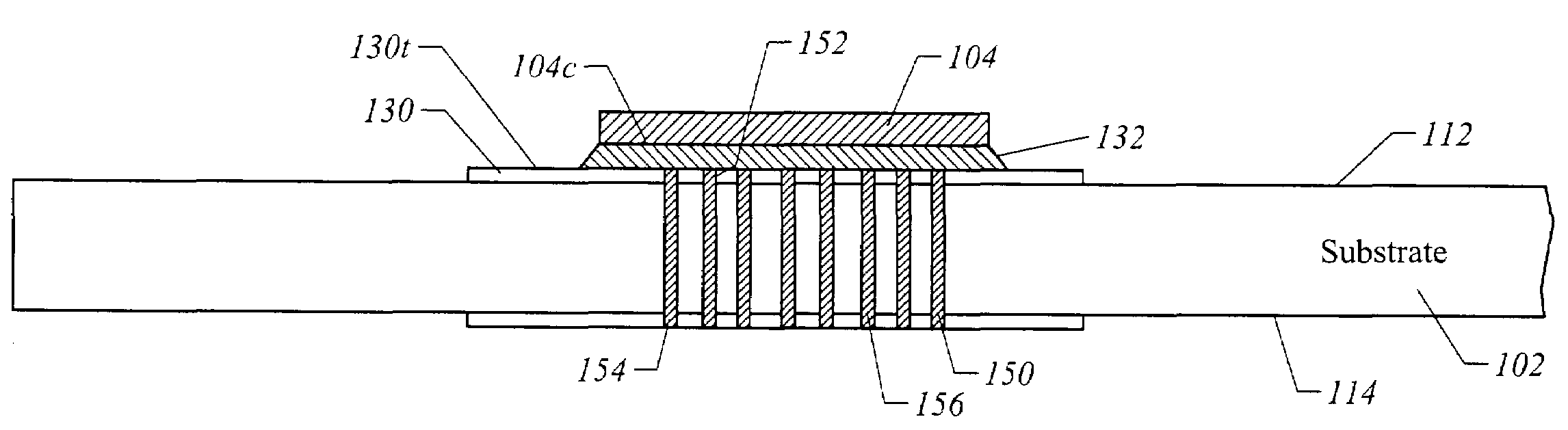
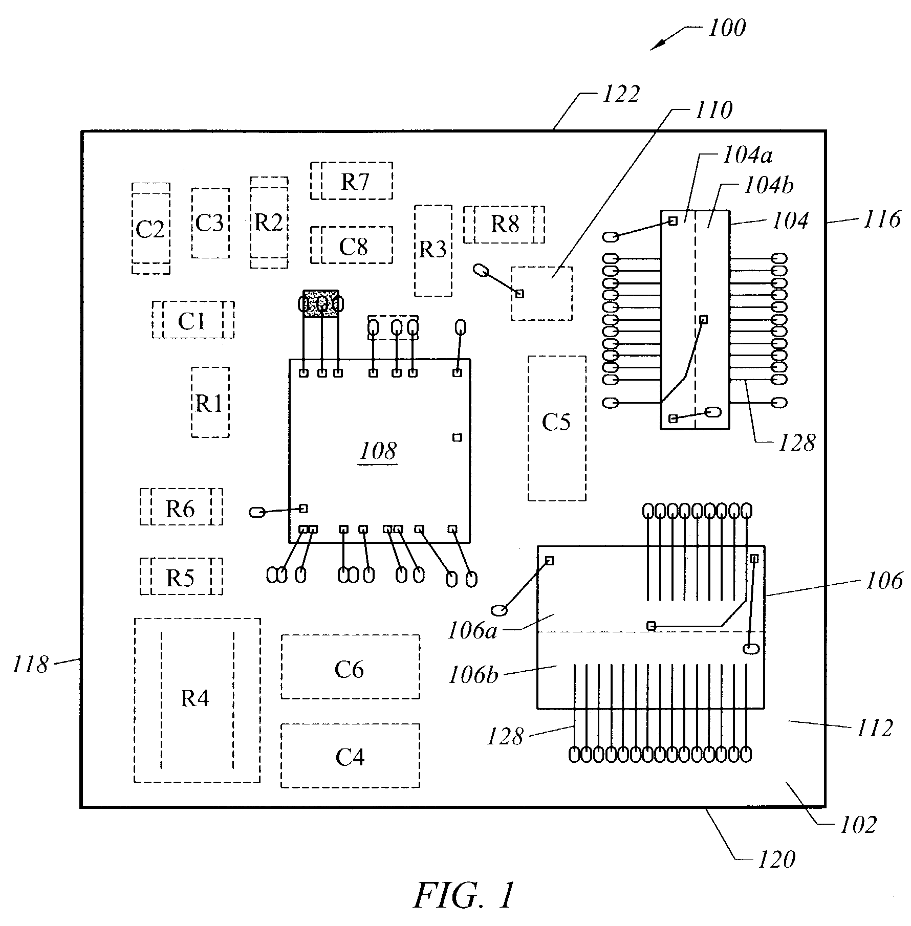
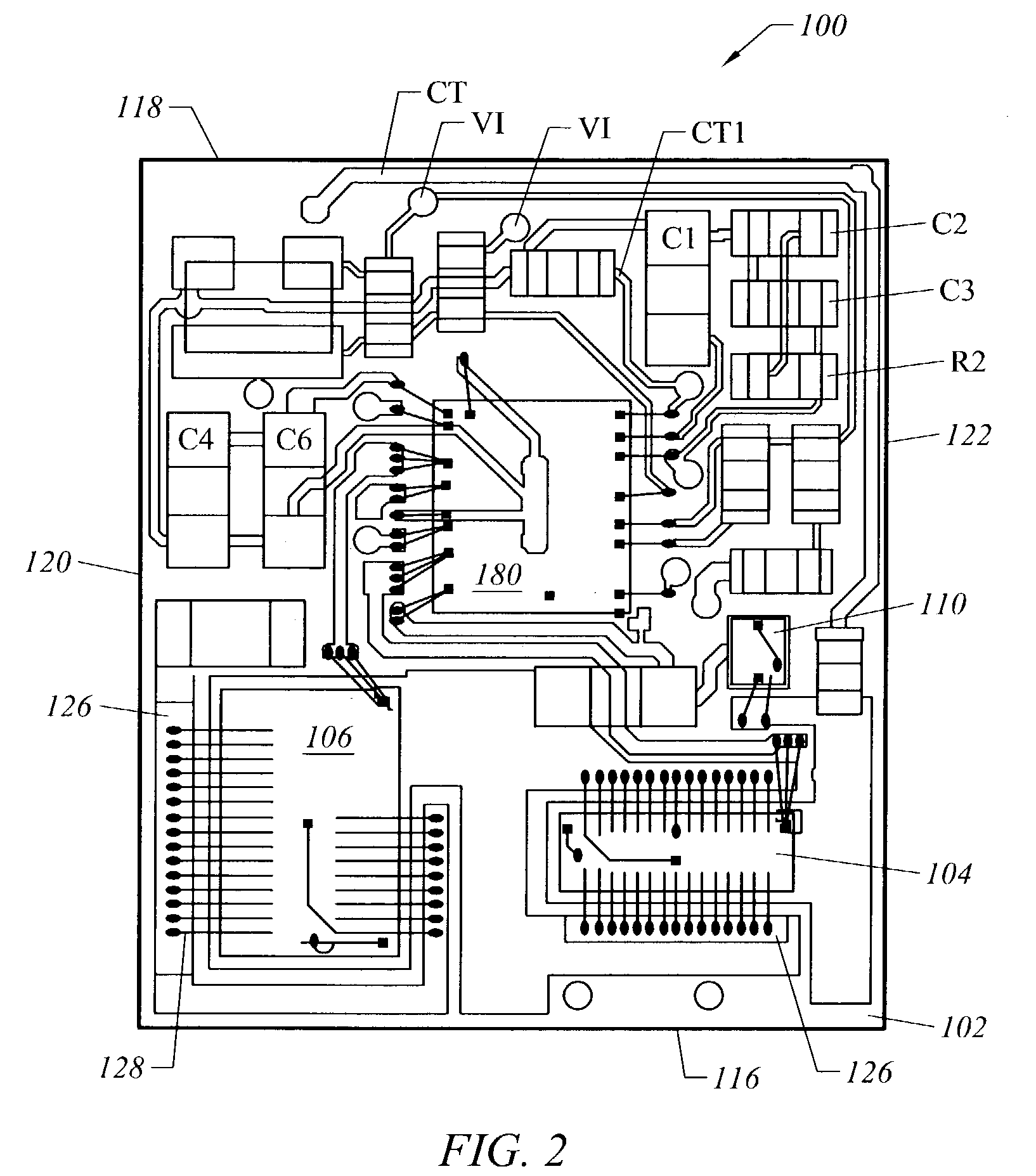
[0020]In general, the present invention integrates a DC—DC converter into an LGA package. FIGS. 1–2 illustrate a top view of a power semiconductor package 100 according to one aspect of the present invention. The power semiconductor package 100 includes, among other components that will be discussed later, a substrate 102, a first power semiconductor die 104, a second power semiconductor die 106, a third semiconductor die 108, a fourth semiconductor die 110, and a plurality of discrete passive components (e.g., resistors R1–R8 and capacitors C1–C9). In a preferred embodiment, the four semiconductor dice 104, 106, 108, 110 and the discrete passive components are electrically coupled together to form a DC—DC converter. The number of discrete passive components mounted on the substrate 102 may vary according to the performance requirements of the package 100. It is also within the scope of the present invention for the package to only contain a portion of a DC—DC converter.

[0021]The su...


PUM


Abstract

A semiconductor chip package that includes a DC—DC converter implemented with a land grid array for interconnection and surface mounting to a printed circuit board. The package includes a two layer substrate comprising a top surface and a bottom surface. At least one via array extends through the substrate. Each via in a via array includes a first end that is proximate to the top surface of the substrate and a second end that is proximate to the bottom surface of the substrate. At least one die attach pad is mounted on the top surface of the substrate and is electrically and thermally coupled to the via array. The DC—DC converter includes at least one power semiconductor die having a bottom surface that forms an electrode. The power semiconductor die is mounted on a die attach pad such that the bottom surface of the die is in electrical contact with the die attach pad. The bottom of the package forms a land grid array. The land grid array includes external pads that are separated into an interior region and a peripheral region. Each external pad located in the interior region of the land grid array is electrically and thermally coupled a via array.

Description

FIELD OF THE INVENTION[0001]The present invention relates generally to a power supply implemented with microelectronic components. More specifically, an embodiment of the present invention integrates a high-current buck regulator into a land grid array (LGA) package in order to provide a regulated voltage.BACKGROUND[0002]Electronic systems face significant challenges for further size reductions, component density and most importantly power density. Many obstacles need to be overcome to meet up to these challenges. Effective heat dissipation and its management coupled with low resistance and low inductance interconnect, combined with the need to provide a low cost package, are but a few of the many barriers.[0003]A conventional power semiconductor package or module includes one or more power semiconductor dies. A power semiconductor die, such as a power MOSFET, has a bottom surface defining a drain contact or electrode, and a top surface that includes a first metallized region defini...

Claims


Application Information

Patent Timeline
Patent Type & Authority Patents(United States)
IPC IPC(8): H01L23/34H01L23/02H01L29/76H01L23/48H01L23/367H02M3/00H02M3/158
CPCH01L23/3677H02M3/1588H02M3/00H01L2224/48227H01L2924/10253H01L2224/73265H01L2924/01055H01L24/49H01L24/48Y02B70/1466H01L2924/3011H01L2924/30107H01L2224/48471H01L2224/49111H01L2924/01077H01L2924/01078H01L2924/13091H01L2924/14H01L2924/19041H01L2924/00H01L2224/05599H01L2224/45099H01L2224/85399H01L2924/00014H01L2224/05554Y02B70/10H02M3/003H01L2224/45015H01L2924/207H01L23/48
Inventor DIVAKAR, MYSORE PURUSHOTHAMKEATING, DAVIDRUSSELL, ANTOIN
Owner BEL POWER SOLUTIONS INC
Why Eureka
Try Eureka