Process options of forming silicided metal gates for advanced CMOS devices

a technology of cmos transistors and metal gates, which is applied in the direction of semiconductor/solid-state device manufacturing, basic electric elements, electric apparatus, etc., can solve the problems of high interface effects, polysilicon resistance related issues, and difficult to achieve metal gate integration in a conventional process flow for cmos transistors, so as to minimize the attack or damage of gate dielectrics

Inactive Publication Date: 2006-04-18
GLOBALFOUNDRIES INC
View PDF5 Cites 53 Cited by
  • Summary
  • Abstract
  • Description
  • Claims
  • Application Information

AI Technical Summary

Problems solved by technology

Throughout the prior art, metal gate integration has proved difficult to achieve in a conventional process flow for CMOS transistors.
This method, however, is highly subject to interface effects and introduces typical polysilicon resistance related issues.
In conventional gate electrodes using polysilicon / silicide, such as Poly-Si / WSix, the increased resistance causes a large gate RC delay, thereby degrading performance.
The current prior art has not sufficiently accounted for unwanted etching of the metal gate surface during cleans or cross-contamination during processing.

Method used


Image

  • Process options of forming silicided metal gates for advanced CMOS devices
  • Process options of forming silicided metal gates for advanced CMOS devices
  • Process options of forming silicided metal gates for advanced CMOS devices

Examples


first embodiment

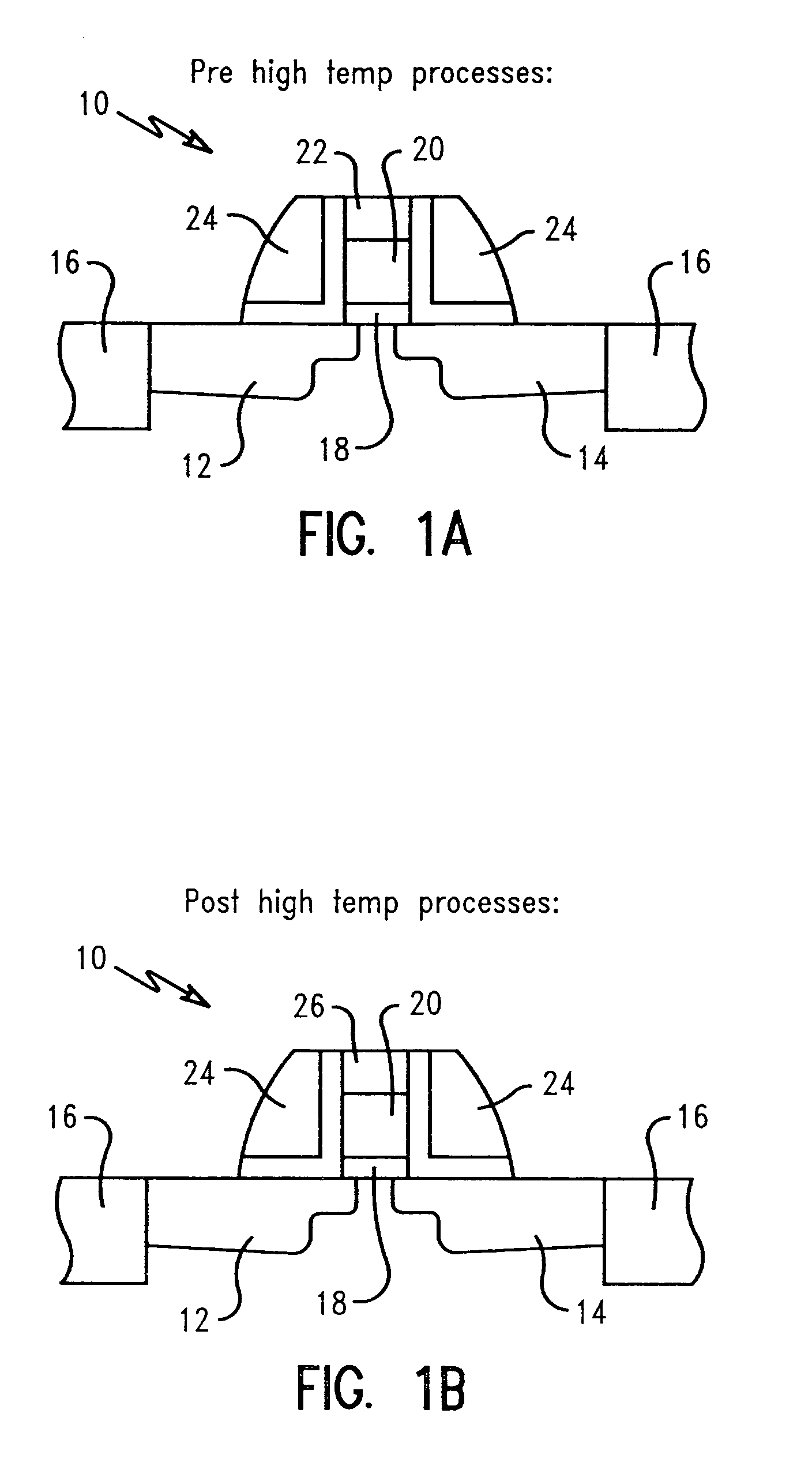
[0050]The gate dielectric 18, metal layer 20, and silicon layer 22 are patterned to define a gate structure having sidewall spacers 24. The patterning may be performed using conventional photolithography and a reactive ion etch (RIE). A polysilicon layer or an oxide film may be used as a hard mask for the patterning of the gate. In this first embodiment, the metal layer 20 is shown to be substantially thicker than the silicon layer 22. FIG. 1B depicts gate 10 after a post high temperature anneal process. Silicon layer 22 is shown transformed into silicide layer 26, forming a cap over the metal layer 20. The formation of the CMOS gate then proceeds in a conventional manner.

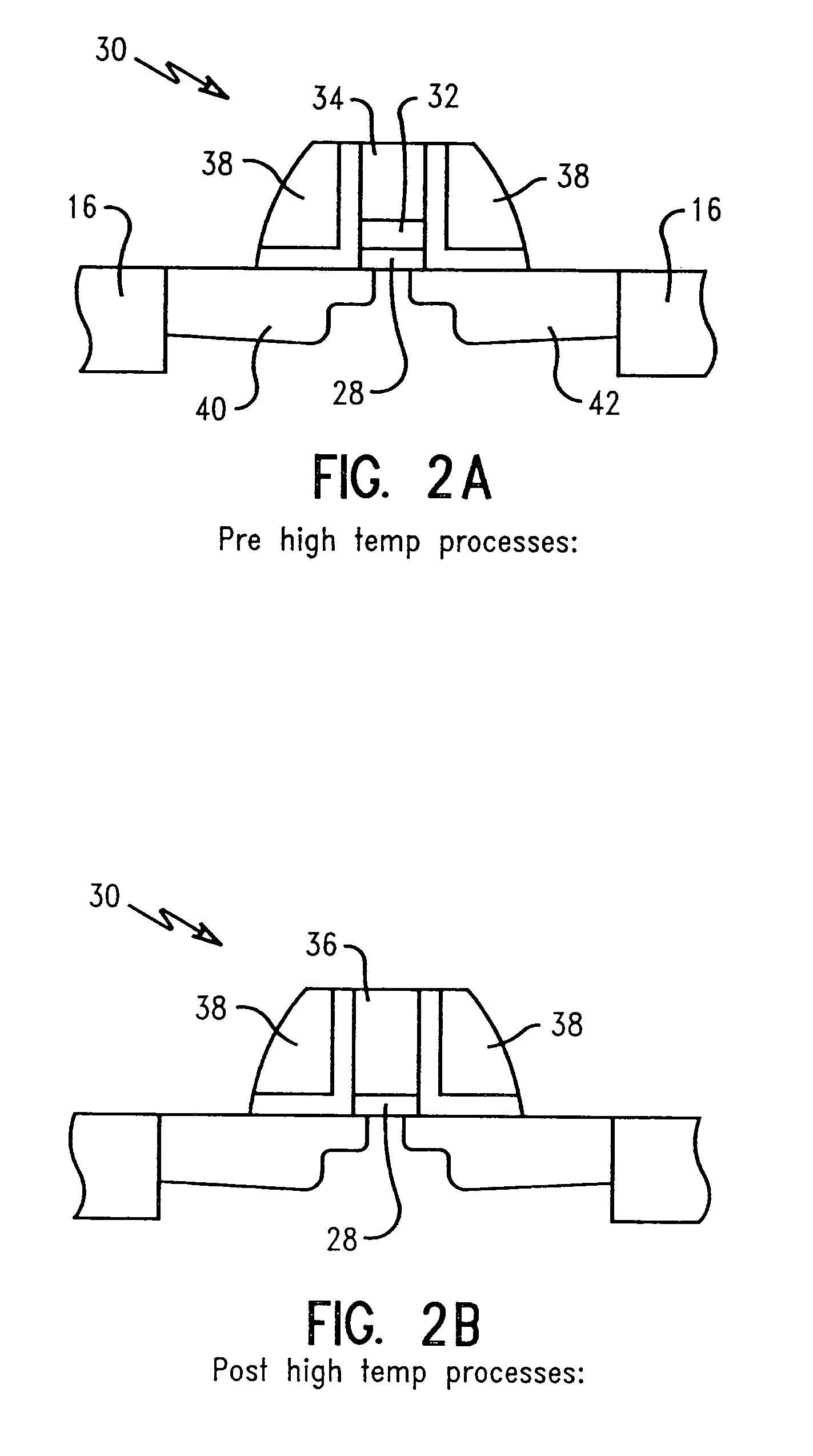
[0051]In a second, similar embodiment, shown in FIG. 2, the silicon layer is deposited at a thickness greater than the metal layer it protects. FIG. 2A depicts a gate structure 30 having a thick polysilicon layer 34 relative to a thin metal layer 32 deposited within the gate prior to annealing. The polysilicon and ...

third embodiment

[0052]In a third embodiment, the gate may optionally have polysilicon sandwiched between two suicides. This configuration depends, in part, upon the overall stack height and layer thickness, among other factors. FIG. 3A depicts a CMOS gate structure 50 having a polysilicon layer fabricated on a metal gate layer. Prior to exposing gate structure 50 to annealing, a silicon layer 52 is deposited on a metal layer 54, which is over a gate dielectric 55. The silicon layer is within a gate structure defined by sidewall spacers 56, source region 58, drain region 60, and shallow trench isolation regions 62. The silicon layer 52 is thick relative to the metal layer 54. After high temperature annealing, a first silicide layer 66, as shown in FIG. 3B, is formed consuming the entire metal gate layer. Important to this embodiment, a second silicide layer 68 may be formed over the polysilicon layer 64. FIG. 3C depicts the post source / drain / gate silicide structure having a polysilicon layer 64 betw...

fourth embodiment

[0053]FIG. 4 depicts, as a fourth embodiment, construction of the metal / silicide gate of the present invention prior to any gate definition. In the pre-silicide formation of FIG. 4A, gate dielectric layer 72, metal layer 74, and silicon layer 76 are deposited over shallow trench isolation regions 78 of substrate 70. The silicon may be deposited using PVD or CVD processes. After high temperature annealing, a silicide layer 80 is formed, as shown in FIG. 4B, over the metal layer 74 and gate dielectric layer 72. Unlike the previously described embodiments, the gate structure is formed after the high temperature process. FIG. 4C depicts a gate 82 formed having sidewall spacers 84, source region 86, and drain region 88, as a post silicide annealing process. In this process the gate metals may comprise Co, W, Mo, Ru, Rh, Re, Ir, and the like. The suicide formed is a reaction of the polysilicon with the gate metal.


PUM


Abstract

Silicide is introduced into the gate region of a CMOS device through different process options for both conventional and replacement gate types processes. Placement of silicide in the gate itself, introduction of the silicide directly in contact with the gate dielectric, introduction of the silicide as a fill on top of a metal gate all ready in place, and introduction the silicide as a capping layer on polysilicon or on the existing metal gate, are presented. Silicide is used as an option to connect between PFET and NFET devices of a CMOS structure. The processes protect the metal gate while allowing for the source and drain silicide to be of a different silicide than the gate silicide. A semiconducting substrate is provided having a gate with a source and a drain region. A gate dielectric layer is deposited on the substrate, along with a metal gate layer. The metal gate layer is then capped with a silicide formed on top of the gate, and conventional formation of the device then proceeds. A second silicide may be employed within the gate. A replacement gate is made from two different metals (dual metal gate replacement) prior to capping with a silicide.

Description

BACKGROUND OF INVENTION[0001]1. Field of the Invention[0002]The present invention relates to the fabrication of integrated circuit devices on semiconductor substrates, and more particularly to CMOS transistor fabrication methods for forming silicided metal gates.[0003]2. Description of Related Art[0004]Throughout the prior art, metal gate integration has proved difficult to achieve in a conventional process flow for CMOS transistors. Most metal gate materials are easily etched when exposed to the standard CMOS cleans for conventional processing, such as sulfuric peroxide (SP) cleans, hydrogen fluoride (HF) etches, and the like. Initial attempts to mitigate this etching concern has centered on capping the metal gate layer with polysilicon. This method, however, is highly subject to interface effects and introduces typical polysilicon resistance related issues. In conventional gate electrodes using polysilicon / silicide, such as Poly-Si / WSix, the increased resistance causes a large gat...

Claims


Application Information

Patent Timeline
Patent Type & Authority Patents(United States)
IPC IPC(8): H01L21/8238H01L21/3205H01L21/4763H01L21/768
CPCH01L21/76895H01L21/823842H01L21/823835
Inventor AMOS, RICKY S.BUCHANAN, DOUGLAS A.CABRAL, JR., CYRILGOUSEV, EVGENI P.KU, VICTORSTEEGEN, AN
Owner GLOBALFOUNDRIES INC
Why Eureka
Try Eureka