Memory data path circuit

a memory data and path circuit technology, applied in the field of memory data path circuits, can solve the problems of large and complex memory devices, high cost of test and repair, and high cost of memory devices, and achieve the effect of easy scaling up and higher compression ratios

Inactive Publication Date: 2006-04-18
WALLER WILLIAM KENNETH
View PDF7 Cites 12 Cited by
  • Summary
  • Abstract
  • Description
  • Claims
  • Application Information

AI Technical Summary

Benefits of technology

[0022]9. a memory read data path compressing data by logical OR, and alternatively logical NOR, of compression data from different memory sections and from the same memory section with no additional wires or controls, providing a design that easily scales up to higher compression ratios.

Problems solved by technology

Memory devices are so large and complex that manufacturing defects are likely to exist in any given device.
The cost of test and repair is a significant portion of the total cost of a memory device.
Using more circuits than necessary has the disadvantages of increasing die size and power consumption, adding wires for interconnect, and causing undesirable differences in electrical parameters, such as additional gate delays, between the circuitry used for testing and that used for normal operation.
The Schicht patent has the further disadvantage of using separate wires to feed out compressed test data and normal mode data, making this design difficult to scale up when adding more memory sections to the compression test scheme.
These non-essential elements have the disadvantages of increasing die size and power consumption without improving performance.
The design disclosed by the Merritt patent has the further disadvantage of requiring added device loading on the data bus lines to support compression.
This added loading inevitably slows down the read cycle.
The Merritt design has the further disadvantage that it is not easily scalable by adding more memory sections to the compression scheme, since it requires more wires when adding more compression circuit blocks.

Method used


Image

  • Memory data path circuit
  • Memory data path circuit
  • Memory data path circuit

Examples


Embodiment Construction

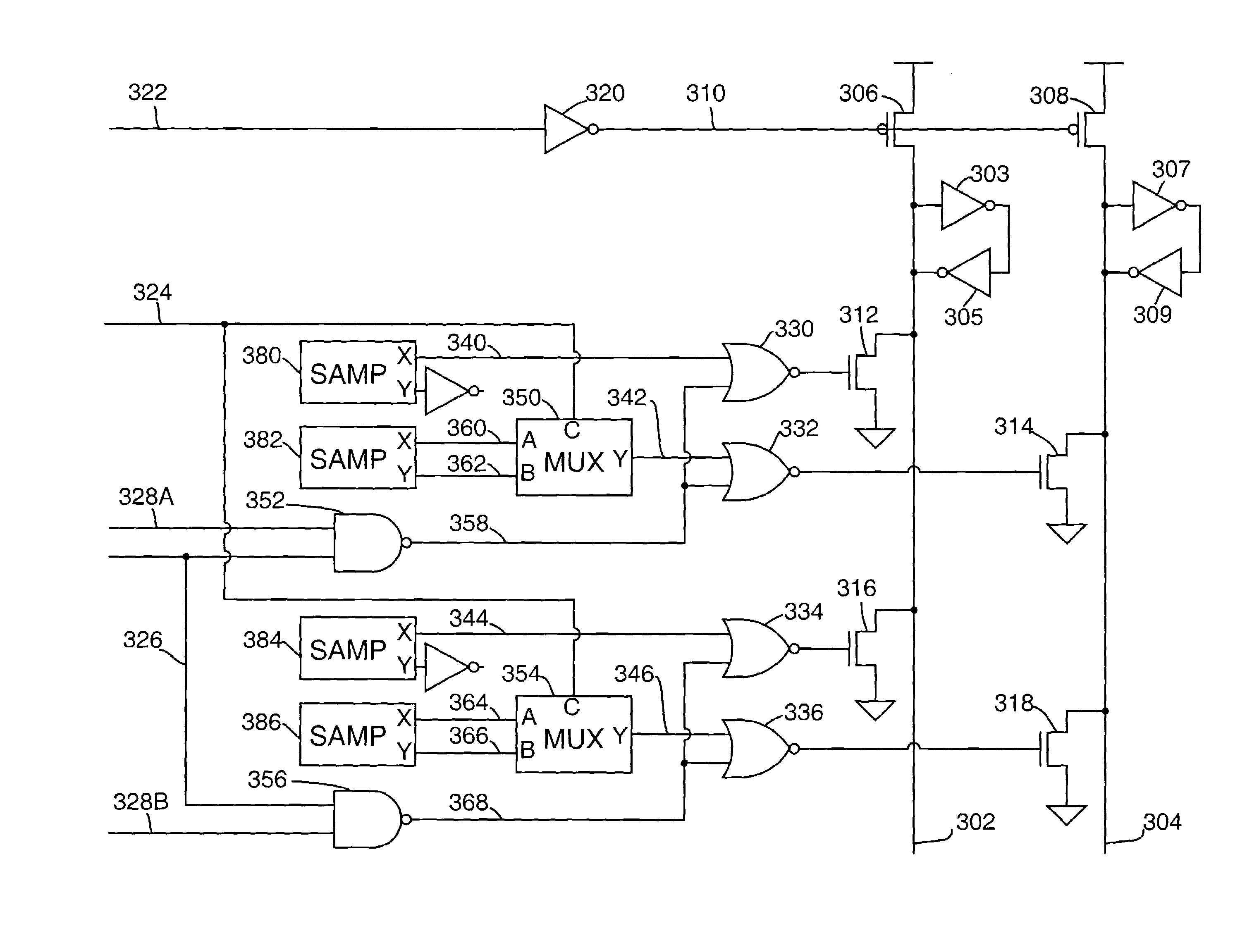
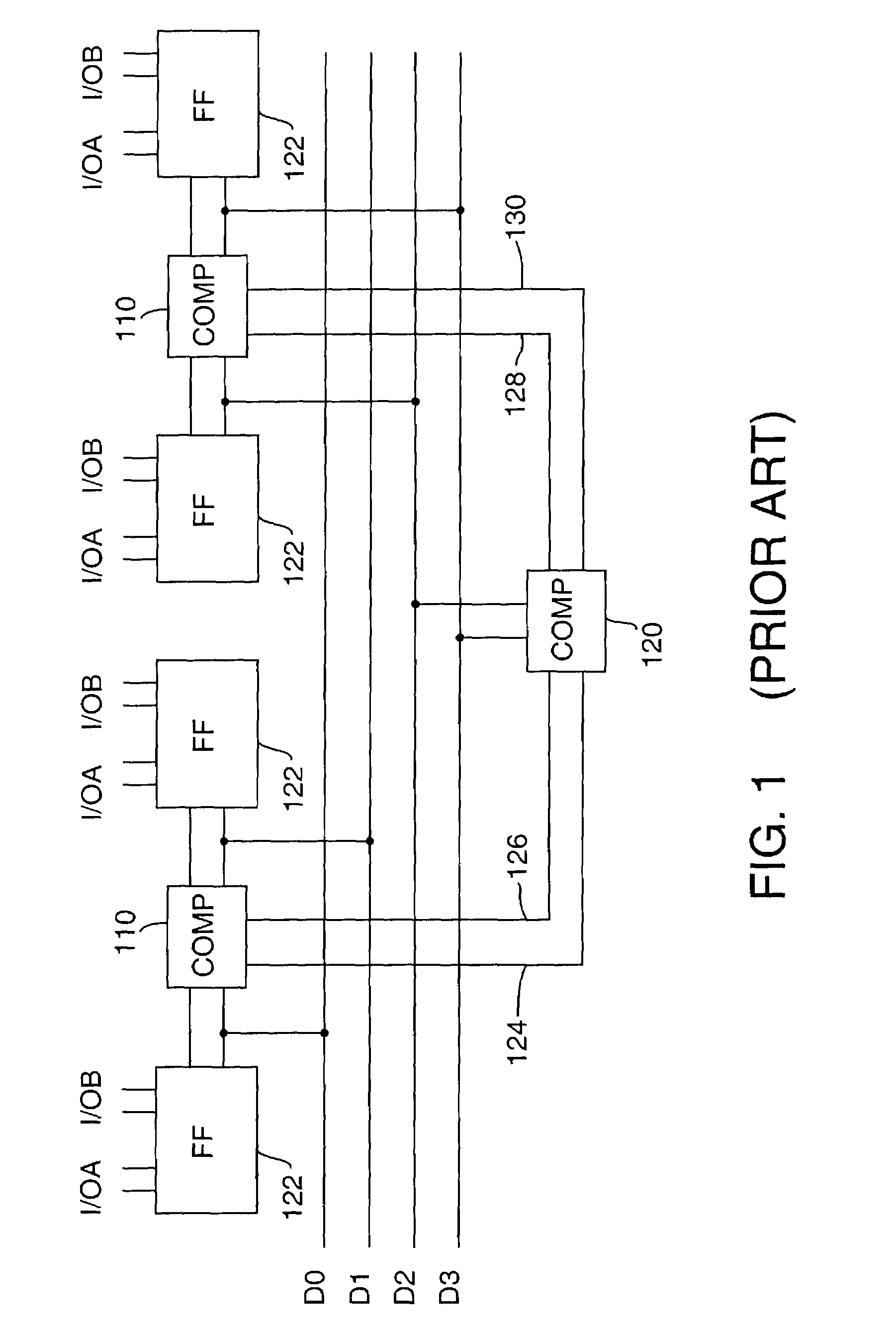
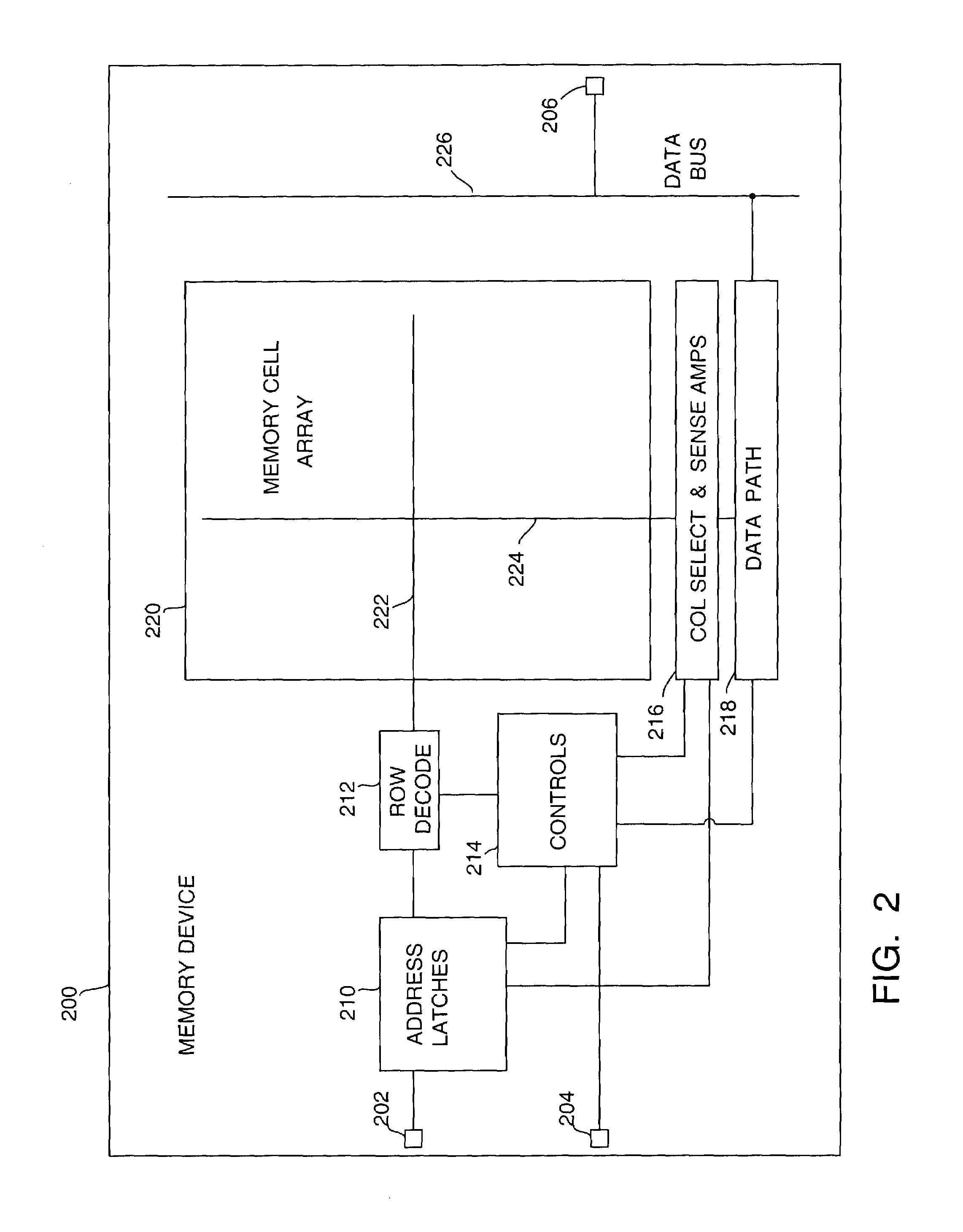
[0028]A memory device 200 as shown in FIG. 2 comprises at least one array of memory cells 220 for retaining data, with support circuitry for reading, writing, and testing. The memory has a write cycle for writing data from external signal ports 206 via data bus 226 to the memory array, and a read cycle for reading data from the array via data bus 226 to the external signal ports. Address latches 210 receive signals from address ports 202, comprising row address, column address, and command data. This information couples to row decoders 212, column select 216, and controls 214, respectively. The controls obtain a reference clock and control signals such as chip-select, read / write, and test from external ports 204, and commands from the address latches to operate row decoders 212, column select 216, and data path circuits 218. Row decoders 212 select a row 222 of memory cells for access, responsive to the row address and section signals from the controls. Column select / sense amplifier...


PUM


Abstract

A memory device with a data path circuit having support in the sense-amp region for compression testing of the device. The data path circuit uses NOR logic compression to provide a scalable design which may be extended to large circuits.

Description

CROSS-REFERENCE TO RELATED APPLICATIONS[0001]Not ApplicableSTATEMENT REGARDING FEDERALLY SPONSORED RESEARCH OR DEVELOPMENT[0002]Not ApplicableREFERENCE TO SEQUENCE LISTING, A TABLE, OR A COMPUTER PROGRAM LISTING COMPACT DISK APPENDIX[0003]Not ApplicableBACKGROUND OF THE INVENTION[0004]The present invention relates to semiconductor memory devices, and more particularly to circuits useful for transferring data into and out from these devices.[0005]Memory devices are so large and complex that manufacturing defects are likely to exist in any given device. Any defects normally require repair after manufacture, by identifying defective portions of a device, and replacing the function of all defective portions with spare circuits built into the device for this purpose. The cost of test and repair is a significant portion of the total cost of a memory device. Data compression methods can minimize time required for test and repair, thus minimizing this cost component.[0006]Data compression i...

Claims


Application Information

Patent Timeline
Patent Type & Authority Patents(United States)
IPC IPC(8): G11C29/00
CPCG11C7/1051G11C29/40G11C7/1069
Inventor WALLER, WILLIAM KENNETH
Owner WALLER WILLIAM KENNETH
Why Eureka
Try Eureka