Mask pattern and method for forming resist pattern using mask pattern thereof

a technology of mask pattern and mask pattern, which is applied in the field of mask pattern and to the method of forming a mask pattern using the mask pattern thereof, can solve the problems of deterioration of meef (mask error enhancement factor), high cost of exposure unit, and reduced exposure wavelength, etc., and achieves excellent resolution and low meef.

Inactive Publication Date: 2006-04-18
SHARP KK
View PDF7 Cites 54 Cited by
  • Summary
  • Abstract
  • Description
  • Claims
  • Application Information

AI Technical Summary

Benefits of technology

[0019]The present invention is provided in view of the above described problems and a purpose thereof is to provide a method for forming a resist pattern according to which the value of MEEF is reduced and, thereby, dispersion in the resist dimensions on a wafer is reduced.
[0022]That is to say, the size of the transmission portion in the mask pattern is greater than that of the resist (space) pattern on a wafer and, therefore, the value of the MEEF can be greatly reduced in photolithography wherein the width is equal to, or smaller than, the wavelength of the exposure light.
[0024]A resist pattern having a low MEEF and an excellent resolution can be formed without a transcription shift by utilizing a conventional unit by means of the mask pattern according to the present invention or by means of a method for forming a resist pattern for carrying out multiple exposures of a semiconductor wafer using such a mask pattern.

Problems solved by technology

However, at present miniaturization of process dimensions tends to be achieved, because of the high cost of exposure units, without further reduction in the wavelength of the exposure light due to progress in miniaturization of factors other than reduction in wavelength and due to super resolution technology such as scanning light exposure technology, illumination formation technology, super resolution mask technology, and the like.
The most critical problem from among these is the deterioration of MEEF (mask error enhancement factor).
That is to say, it is understood that the fluctuation in the angle of diffraction corresponds to change in space size and is great resulting in deterioration in the value of MEEF because space size is small in comparison with the wavelength.
In recent years, the reduction in this MEEF value has become an important issue for photolithography that implements process dimensions of the wavelength of the exposure light, or less.

Method used


Image

  • Mask pattern and method for forming resist pattern using mask pattern thereof
  • Mask pattern and method for forming resist pattern using mask pattern thereof
  • Mask pattern and method for forming resist pattern using mask pattern thereof

Examples


Embodiment Construction

[0034]The mask pattern according to the present invention may be formed of a metal such as chrome or silicon.

[0035]The aperture pattern for forming the mask pattern may be formed using a halftone mask or a Levenson mask that becomes a phase shifter. In that case, light contrast at the time of transcription increases and, at the same time, the value of MEEF is reduced.

[0036]The light-shielding pattern for forming the mask pattern is formed using a binary mask made of chrome or a halftone mask made of MoSiO. In that case, the light contrast increases at the time of transcription and, at the same time, the value of the MEEF is reduced.

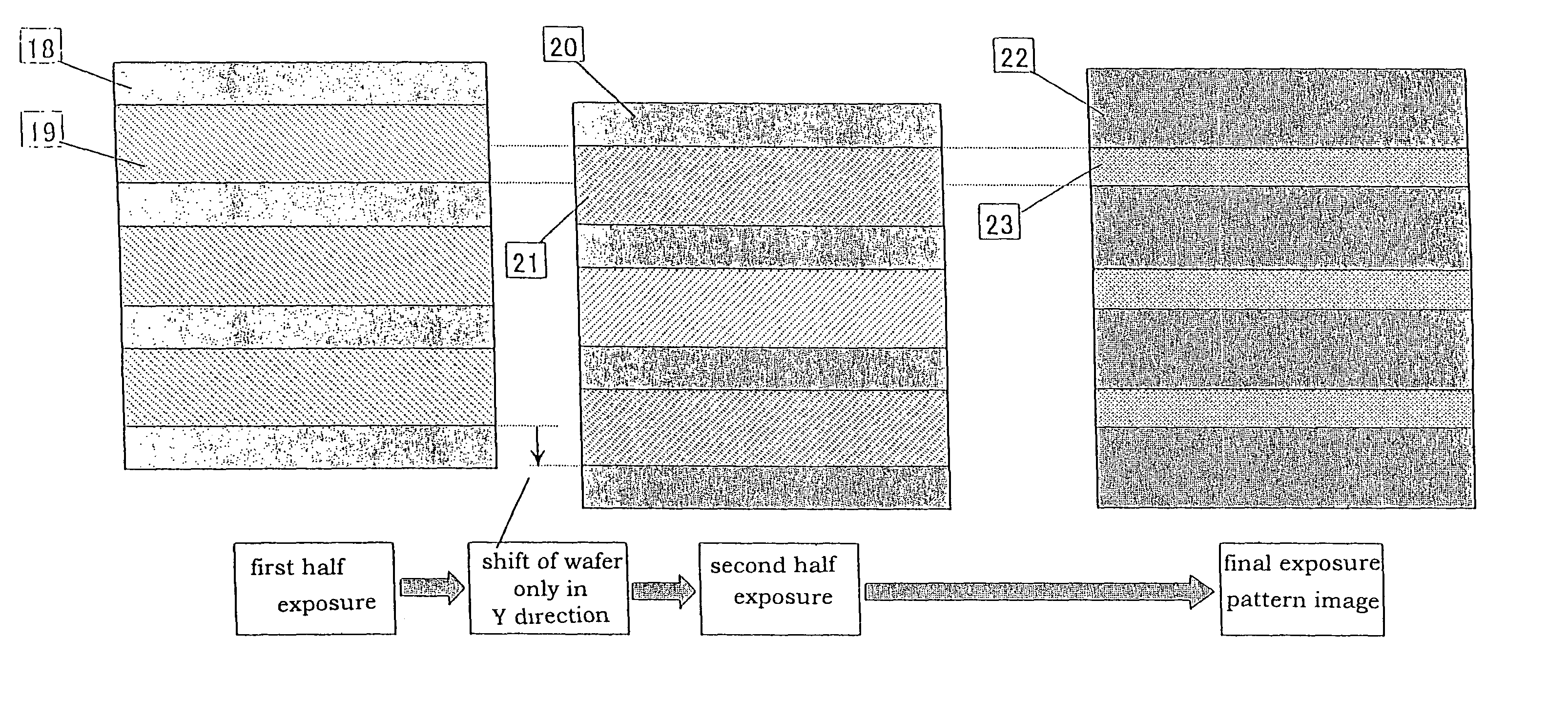
[0037]The “case where a mask pattern under a design having the width of an aperture pattern smaller than the width of a light-shielding pattern is used at one exposure” in the present invention indicates the case wherein the width (line width) of the aperture pattern is less than 100% of the width (space width) of the light-shielding pattern.

[0038]The “wi...


PUM

PropertyMeasurementUnit
wavelengthaaaaaaaaaa

Abstract

A mask pattern for multiple exposure for forming a resist pattern with an unvarying pattern pitch on a semiconductor wafer, which is utilized as in case where a mask pattern under a design having the width of an aperture pattern smaller than the width of a light-shielding pattern is used at one exposure, wherein the mask pattern for multiple exposure has a pattern pitch that is the same as that of the mask pattern under design and has the width of an aperture pattern greater than the width of a light-shielding pattern.

Description

CROSS-REFERENCE TO RELATED APPLICATION[0001]This application is related to Japanese application No. 2002-226275 filed on Aug. 2, 2002, whose priority is claimed under 35 USC § 119, the disclosure of which is incorporated by reference in its entirety.BACKGROUND OF THE INVENTION[0002]1. Field of the Invention[0003]The present invention relates to a mask pattern and to a method for forming a resist pattern using the mask pattern thereof, in particular relates to a mask pattern wherein the amplification ratio of mask CD (critical dimension: minimum dimension) dispersion at the time of transcription to a wafer by means of exposure is reduced so that the mask pattern contributes to an increase in the precision of a resist CD in the formation of a resist pattern, and relates to a method for forming a resist pattern using the mask pattern thereof.[0004]2. Description of the Background Art[0005]In recent years, miniaturization of resist patterns has greatly been dependant on progress in phot...

Claims


Application Information

Patent Timeline
Patent Type & Authority Patents(United States)
IPC IPC(8): G06F17/50G03F1/00G03F1/14G03F1/30G03F1/32G03F1/68G03F7/20H01L21/027
CPCG03F1/30G03F7/203G03F1/32
Inventor KOBAYASHI, SHINJI
Owner SHARP KK
Why Eureka
Try Eureka