Method for chemical-mechanical jet etching of semiconductor structures

a technology of chemical mechanical jet etching and semiconductor structure, which is applied in the direction of spray nozzles, basic electric elements, decorative arts, etc., can solve the problems that the etch rate achievable by such methods is generally too low to be practical in commercial production, and achieves rapid and accurate removal of large amounts of material, high etching efficiency, and high etching efficiency.

Inactive Publication Date: 2006-05-02
APPLIED MATERIALS INC
View PDF31 Cites 39 Cited by
  • Summary
  • Abstract
  • Description
  • Claims
  • Application Information

AI Technical Summary

Benefits of technology

[0006]We have invented a chemical-mechanical jet etching method which is capable of quickly and accurately removing large amounts of material from a workpiece in wafer thinning applications, and is capable of rapidly producing large-scale features, with critical dimensions on the order of 1–100 microns, and aspect ratios (defined as the ratio of the depth of an etched feature to the maximum diameter of a via, or the maximum width of a trench, at the entrance) in the range of 1:1 to 10:1. The method of the invention can be carried out on a generally flat semiconductor workpiece, including but not limited to a silicon wafer or gallium arsenide or other semiconductor substrate, silicon-on-insulator (“SOI”), SiO2, glass, quartz, pyrex, ceramic, or glass bonded to a substrate, conductor, or insulator. In particular, the method is expected to function very advantageously when applied to silicon wafer, gallium arsenide, and SOI substrates, In both thinning and feature creation applications, etch rates of at least about 10–100 microns of substrate thickness per minute can be achieved.

Problems solved by technology

Where the required features are relatively large-scale, in the range of from about 10 to about 100 microns, as in making a through-wafer via or large trench on a silicon wafer, or the amount of material to be removed is large, as in wafer thinning applications, and the required precision is less critical, the etch rates achievable by such methods are generally too low to be practical in commercial production.

Method used


Image

  • Method for chemical-mechanical jet etching of semiconductor structures
  • Method for chemical-mechanical jet etching of semiconductor structures
  • Method for chemical-mechanical jet etching of semiconductor structures

Examples


example 1

Thinning

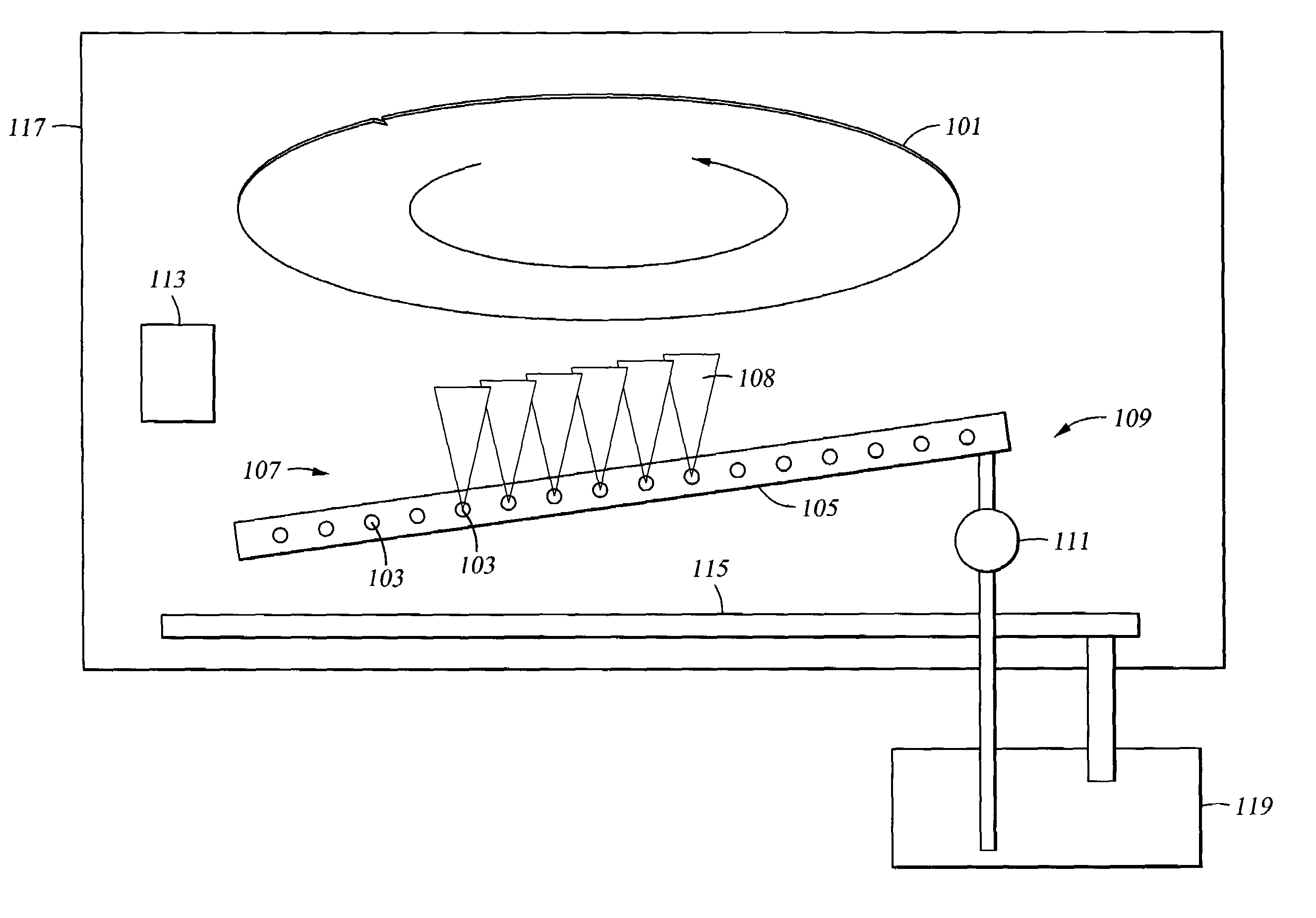
[0021]In a first embodiment of the invention, a silicon wafer, other semiconductor substrate, or other workpiece, is uniformly thinned by using the apparatus shown in FIG. 1.

[0022]A workpiece (not shown) is affixed to the workpiece holder 101, and the holder 101 rotates the workpiece beneath the injector bar 105, with its array 107 of high-pressure nozzles 103. A machining etchant, in the form of a slurry or suspension of appropriate particulate material in a chemical etchant / solvent, in a concentration in the range of from about zero to about 95 weight percent, is pumped by pump 111 through delivery system 109 to nozzle array 107 on injector bar 105, at a nozzle pressure in the range of about 7 to about 70 Kg / cm2. Nozzles 103 then deliver the machining etchant 108 as a high-pressure jet which impinges upon the workpiece wafer as the holder 101 and workpiece rotate past the nozzles 103 at a speed ranging from about 100 to about 2000 RPM.

[0023]The angle at which the machining...

example 2

Patterning

[0028]A second embodiment of the invention uses the same the general apparatus as is illustrated by FIG. 1, and operation as described in Example 1, but utilizes a patterned mask applied to the surface of the semiconductor workpiece to permit selective etching of a surface of that workpiece. Relatively large-scale features, such as trenches and vias with critical dimensions in the range of from about 5 to several hundred microns, and depths of up to the full thickness of the workpiece wafer, can be readily produced in this way, again at etch rates as high as about 100 microns of depth per minute. Typical process conditions for this embodiment of the method of the invention are also as presented in Table I, above.

[0029]The patterned mask may consist of either a conventional organic photoresist, or a glasslike silane material, or an inorganic hard mask, such as silicon oxide or silicon nitride, which are generally known in the art.

[0030]This chemical-mechanical jet etch meth...

example 3

Maskless Jet Etching.

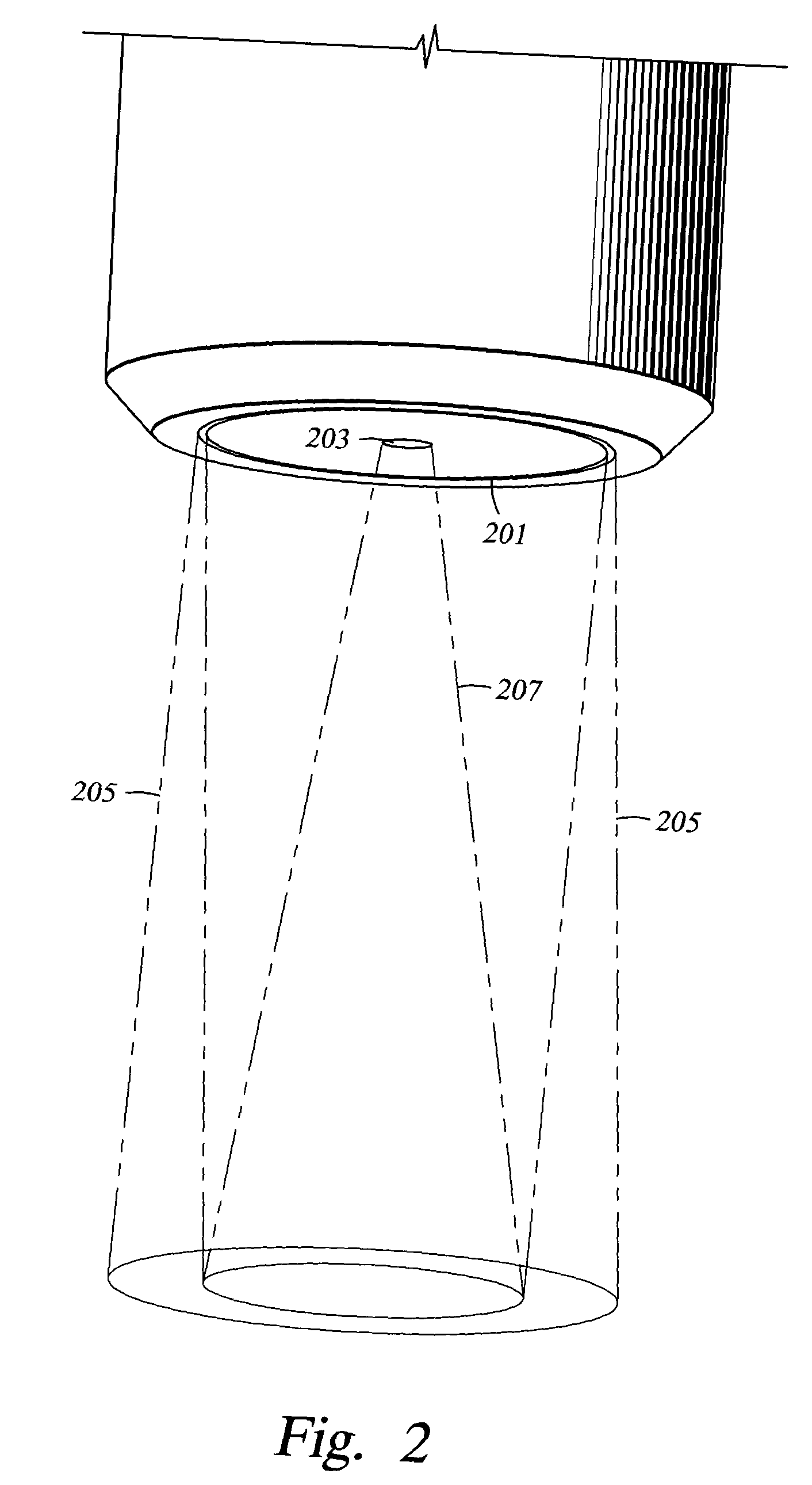
[0033]A third embodiment of the invention again uses the basic apparatus illustrated in FIG. 1, but, as in the wafer thinning operations described in Example 1, uses no mask. Instead, in this embodiment, intended for making multiple vias in or through a silicon wafer or other semiconductor workpiece, the workpiece is held stationary, and a narrow stream of machining etchant is directed, from a single narrowly-focused nozzle, at each desired via location, serially with one nozzle or concurrently with multiple nozzles, until the desired etch depth is achieved. Pulsed delivery of machining etchant, as described above, may be advantageous to avoid buildup of machining etchant loaded with etched material, or stagnation of the etchant, in the hole. Process conditions are again generally those shown in Table 1. Features in the size range of about 10 μ or larger can be direct-written in this way.

[0034]The narrowly-focused machining etchant stream of this embodiment may ...


PUM

PropertyMeasurementUnit
thicknessaaaaaaaaaa
diameteraaaaaaaaaa
thicknessaaaaaaaaaa

Abstract

A chemical-mechanical jet etching method rapidly removes large amounts of material in wafer thinning, or produces large-scale features on a silicon wafer, gallium arsenide substrate, or similar flat semiconductor workpiece, at etch rates in the range of 10–100 microns of workpiece thickness per minute. A nozzle or array of nozzles, optionally including a dual-orifice nozzle, delivers a high-pressure jet of machining etchant fluid to the surface of the workpiece. The machining etchant comprises a liquid or gas, carrying particulate material. The liquid may be a chemical etchant, or a solvent for a chemical etchant, if desired. The areas which are not to be etched may be shielded from the jet by a patterned mask, or the jet may be directed at areas from which material is to be removed, as in wafer thinning or direct writing, depending on the size of the desired feature or etched area.

Description

[0001]This application is a divisional application of U.S. application Ser. No. 09 / 932,396, filed Aug. 17, 2001, which issued as U.S. Pat. No. 6,699,356 on Mar. 2, 2004.BACKGROUND OF THE INVENTION[0002]1. Field of the Invention[0003]This invention relates to a method and an apparatus for achieving chemical-mechanical jet etching of features in a workpiece such as a semiconductor substrate or a built-up stack of films. In particular, the invention permits high etch rates for thinning the workpiece or for production of relatively large dimension etched features in such a workpiece, such as trenches and through-wafer vias for electrical contacts, or reservoirs for ink-jet heads, where critical dimensions are relatively large, on the order of 1–100 microns, or for thinning in the range of 100–1000 microns.[0004]2. Brief Description of the Background Art[0005]Various wet-chemical etching, dry-etching (i.e., various forms of plasma etching) and electrochemical methods exist which permit c...

Claims


Application Information

Patent Timeline
Patent Type & Authority Patents(United States)
IPC IPC(8): H01L21/302B05B1/20B05B7/06B05B7/08H01L21/00
CPCH01L21/6708B05B1/20B05B7/0884B05B7/06
Inventor BACHRACH, ROBERT Z.CHINN, JEFFREY D.
Owner APPLIED MATERIALS INC
Why Eureka
Try Eureka