Semiconductor integrated circuit device

a technology of integrated circuits and semiconductors, applied in the field of semiconductor devices, can solve the problems of reducing product yield and failure of signal distribution systems, and achieve the effects of enhancing data transfer rate, reducing the number of wirings that pass through the chip center for impedance control, and reducing the probability of cord blowing failur

Inactive Publication Date: 2006-05-02
RENESAS ELECTRONICS CORP
View PDF9 Cites 80 Cited by
  • Summary
  • Abstract
  • Description
  • Claims
  • Application Information

AI Technical Summary

Benefits of technology

[0007]In a semiconductor device, the output impedance may be adjusted so as to become equal to the resistance value of a resistive element. However, in such an embodiment, a relatively large number of control signals may be required to adjust, or control, the resistance value with sufficiently high accuracy. For example, in order to control impedance of 27 types, for example, P channel N channel MOSFETs, respectively, necessitate control signals of 7 bits. For a 7 bit control signal, it would be necessary to provide 7×2=14 signal lines. In order to provide terminating circuits to perform the impedance control discussed hereinabove, large numbers of wirings are necessitated. In a semiconductor integrated circuit device, such as a memory, a great many signals are concentrated, and hence extra wiring channels are required to pass the many signals to the terminating circuits. In such a configuration, signal lines and channels may be distributed over the entire semiconductor chip on which the semiconductor device is resident, and thus the probability of failure in the signal distribution system increases in a complex semiconductor device, thereby correspondingly reducing product yield.
[0008]The present invention provides a semiconductor integrated circuit device equipped with an impedance control circuit. More specifically, the present invention provides a semiconductor integrated circuit device that is simplistic in use and that enhances data transfer rate.
[0012]Thus, the number of wirings that pass through a chip center for impedance control are reduced by the present invention, and the probability of a cord-blown failure due to foreign materials and breaks with respect to the number of wirings is thus also reduced. and the present invention also enhances a data transfer rate over a system.

Problems solved by technology

In such a configuration, signal lines and channels may be distributed over the entire semiconductor chip on which the semiconductor device is resident, and thus the probability of failure in the signal distribution system increases in a complex semiconductor device, thereby correspondingly reducing product yield.

Method used


Image

  • Semiconductor integrated circuit device
  • Semiconductor integrated circuit device
  • Semiconductor integrated circuit device

Examples


Embodiment Construction

[0043]It is to be understood that the figures and descriptions of the present invention have been simplified to illustrate elements that are relevant for a clear understanding of the present invention, while eliminating, for purposes of clarity, many other elements found in a typical semiconductor device and method. Those of ordinary skill in the art will recognize that other elements are desirable and / or required in order to implement the present invention. But because such elements are well known in the art, and because they do not facilitate a better understanding of the present invention, a discussion of such elements is not provided herein. The disclosure herein is directed to all such variations and modifications to the applications, networks, systems and methods disclosed herein and as will be known, or apparent, to those skilled in the art.

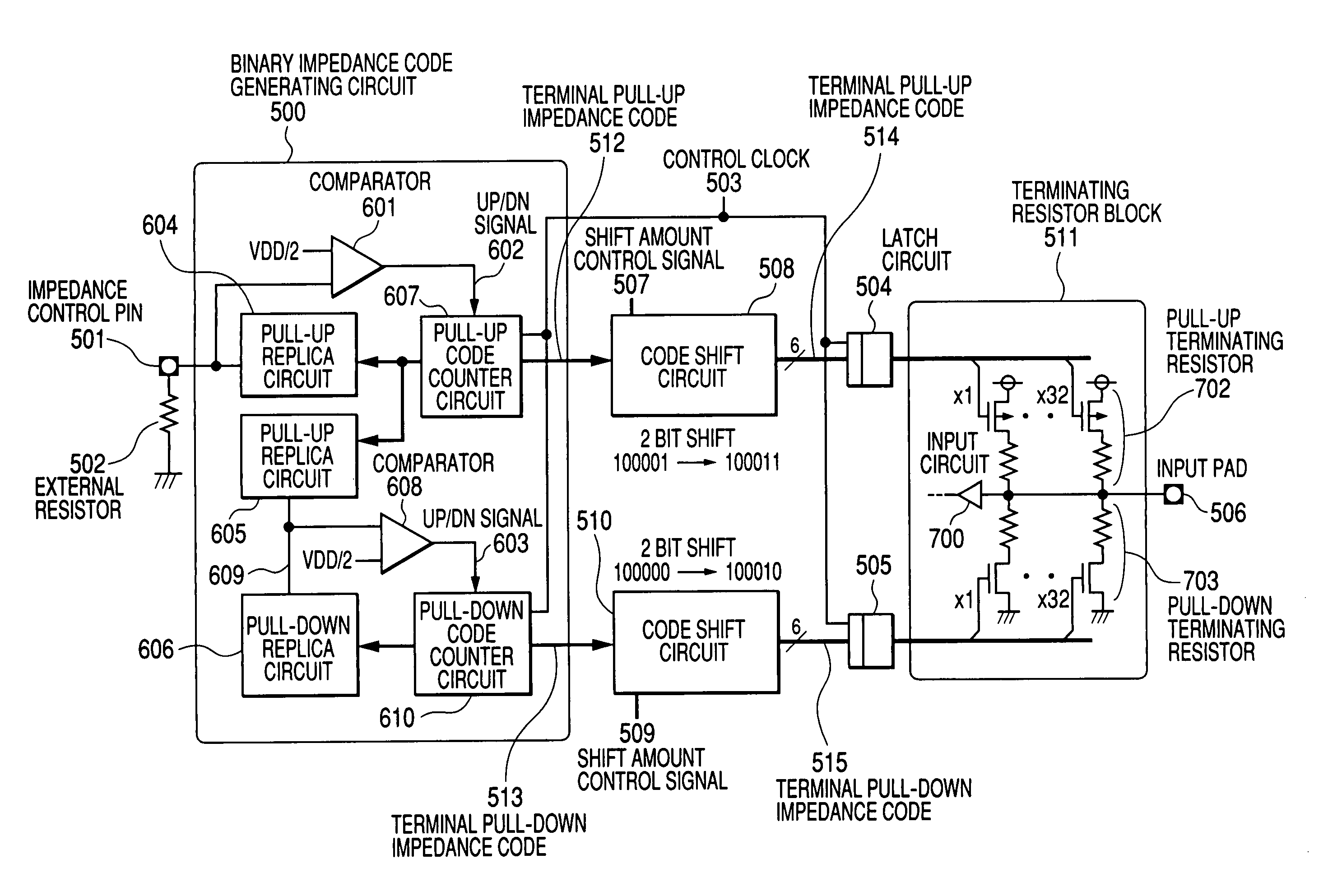
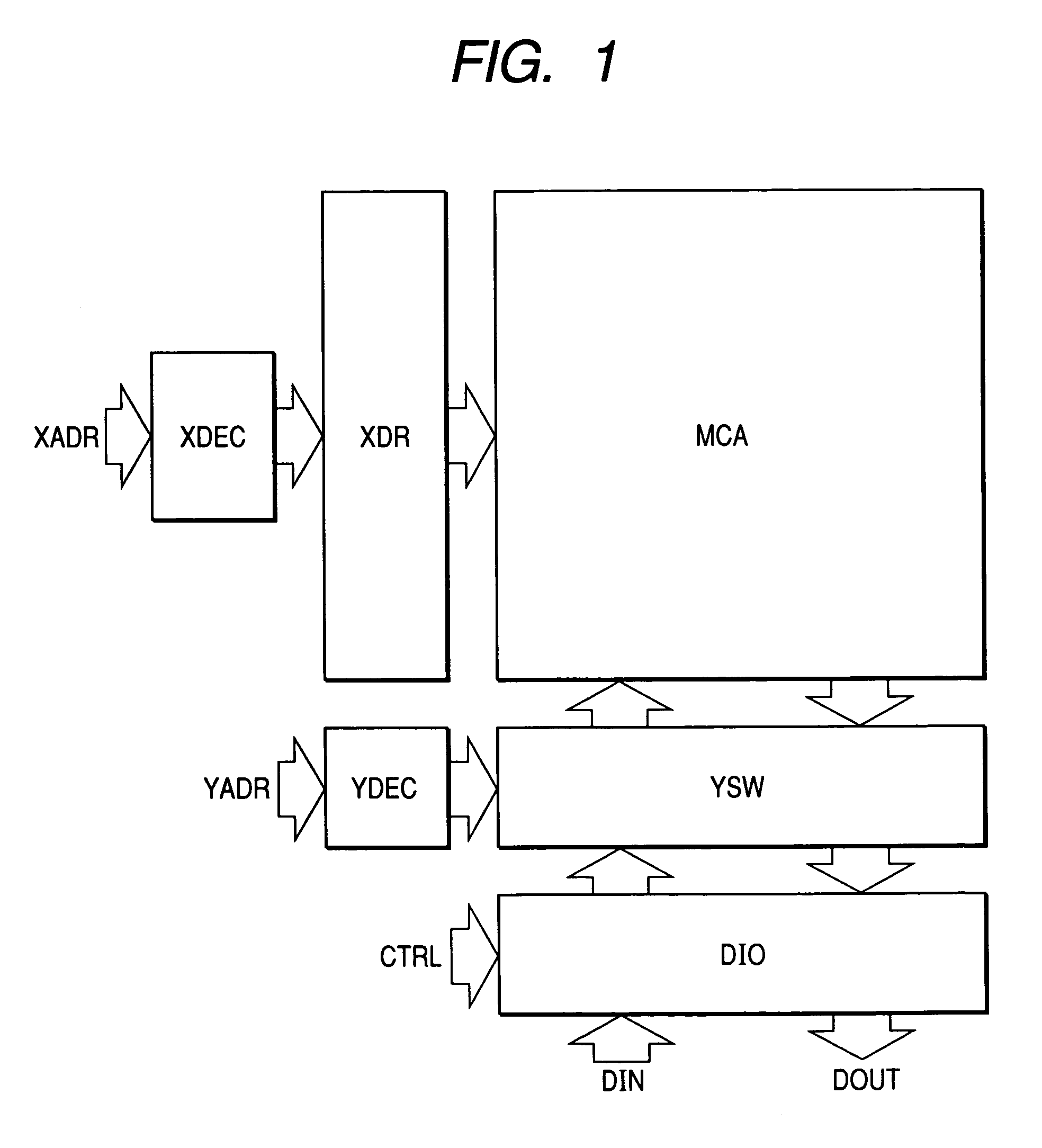
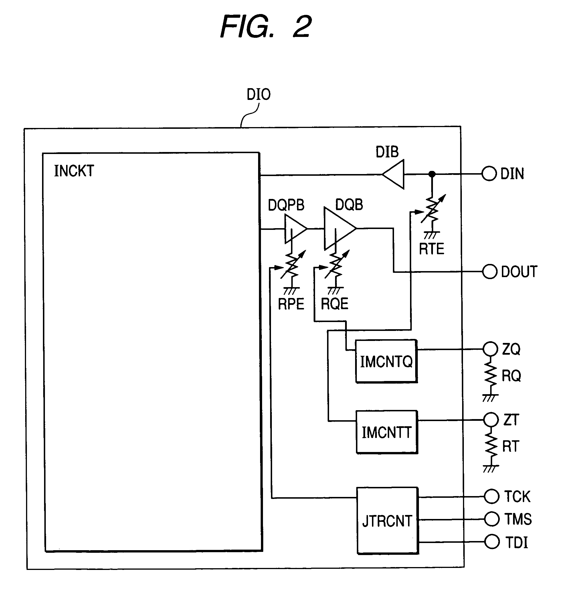
[0044]A block diagram of an embodiment of a semiconductor memory related to the present invention is shown in FIG. 1. XADR is a row addre...


PUM


Abstract

A plurality of sets of circuits are provided, each of which generates an impedance code through the use of an impedance control circuit in association with a resistive element connected to an external terminal, and each of which varies the impedance in accordance with such an impedance code. The impedance control circuit includes an impedance comparator which is formed equivalently to the resistive element and the plurality of sets of circuits, and which performs an impedance comparison with each of a plurality of replica circuits to form an up signal that increases the impedance and a down signal that decreases the impedance. Counters are provided adjacent to the individuals of the plurality of sets of circuits to thereby generate the impedance codes in response to the up signal and the down signal.

Description

CROSS-REFERENCE TO RELATED APPLICATION[0001]The present application claims priority from Japanese patent application JP 2003-274771, filed on Jul. 15, 2003, the contents of which are hereby incorporated by reference as if set forth in the entirety herein.FIELD OF THE INVENTION[0002]The present invention relates to a semiconductor device, and, more specifically, to a method, system, and device for data transfer at high frequency.BACKGROUND OF THE INVENTION[0003]In order to perform the transfer of data between a memory LSI (Large Scale Integration) and a MPU (Microprocessor) or the like at high speed (high frequency), it is necessary to impedance match the transmission system and to suppress distortion of the transfer waveform caused by reflection. It is known to control the impedance of the output driver of a high-speed synchronous SRAM (Static Random Access Memory) so as to provide an impedance equal to the resistance value of a resistive element connected to a dedicated LSI pin, fo...

Claims


Application Information

Patent Timeline
Patent Type & Authority Patents(United States)
IPC IPC(8): H03K19/003H03K19/0175G11C7/00H03H11/28H03H11/30H03K5/22H03K17/16H03K19/00H04L25/02
CPCH04L25/0278H03H11/30G11C7/1051H03K19/0005
Inventor AOYAMA, SATOSHIHAYASHI, ATSUHIROTAKAHASHI, YASUHIKO
Owner RENESAS ELECTRONICS CORP
Why Eureka
Try Eureka