Static semiconductor memory device having T-type bit line structure

a semiconductor memory and bit line technology, applied in semiconductor devices, digital storage, instruments, etc., can solve the problems of /bl narrowing the interval between lines of the bit line pair bl, sram has been decreased, memory cells have lost popularity, etc., and achieves a small layout area and high operation rate.

Inactive Publication Date: 2006-05-02
RENESAS TECH CORP
View PDF11 Cites 6 Cited by
  • Summary
  • Abstract
  • Description
  • Claims
  • Application Information

AI Technical Summary

Benefits of technology

[0021]Accordingly, a main object of the present invention is to provide a static semiconductor memory device whose layout area is small and whose operation rate is high.
[0022]A static semiconductor memory device according to the present invention is provided with a number M×N of memory blocks which are arranged in M rows by N columns and each of which include a number 8×M of horizontal memory cells arranged in 8 rows by M columns, M×N pairs of first and second bit line signal input / output lines, M sets of first and second data input / output lines, first and second power supply lines, global word lines and global column selecting lines, a selection circuit responsive to an address signal for selecting one of the number M×N of memory blocks and one of the number 8×M of memory cells belonging to the selected memory block, a write / read circuit and a gate circuit for coupling a memory cell selected by the selection circuit to the write / read circuit, in which in each memory block, the above-described eight lines are arranged above eight memory cell rows of the memory block and the first and the second power supply lines are arranged between the global word line and the global column selecting line, and the remaining four lines, respectively. Accordingly, since it is only necessary to provide one line above one memory cell row, an SRAM having the T-type bit line structure can be formed with ease using a horizontal memory cell, which enables reduction in a layout area and speed-up of an operation rate. In addition, since the first and the second power supply lines are arranged between the global word line and the global column selecting line for transmitting a high amplitude signal, and the other four lines for transmitting a low amplitude signal, coupling noise between the lines can be reduced.

Problems solved by technology

These memory cells, however, have lost their popularities as a power supply voltage of an SRAM has been decreased from 3 V to 2.5 V, 1.8 V and down to 1.5 V because they are not excellent in low-voltage operation characteristics, while a full CMOS cell having six transistors excellent in low-voltage operation characteristics is gaining a popularity.
In a conventional SRAM, however, since a bit line load circuit, a sense amplifier, a gate circuit and a fuse concentrate on an end portion of the bit line pair BL, / BL narrowing an interval between lines of the bit line pair BL, / BL is difficult.

Method used


Image

  • Static semiconductor memory device having T-type bit line structure
  • Static semiconductor memory device having T-type bit line structure
  • Static semiconductor memory device having T-type bit line structure

Examples


Embodiment Construction

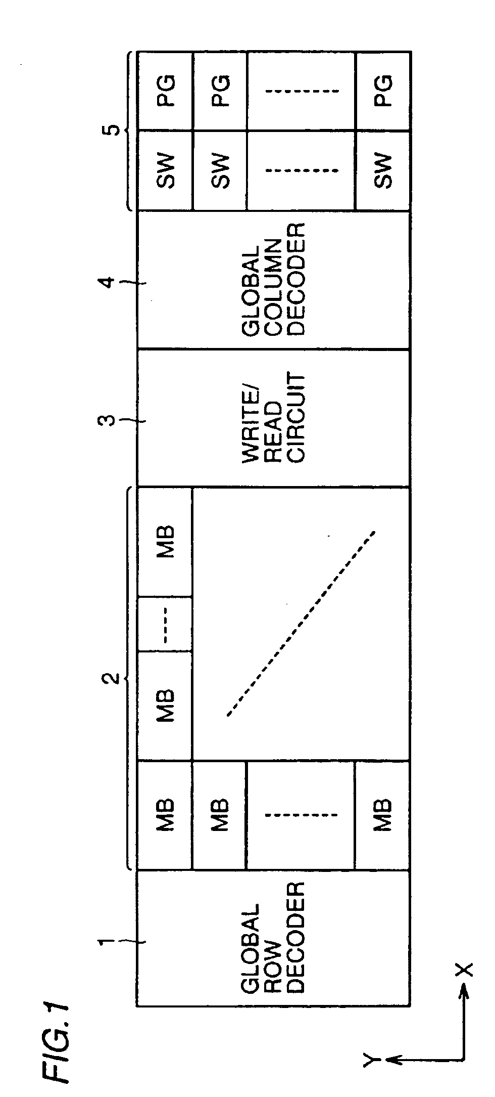
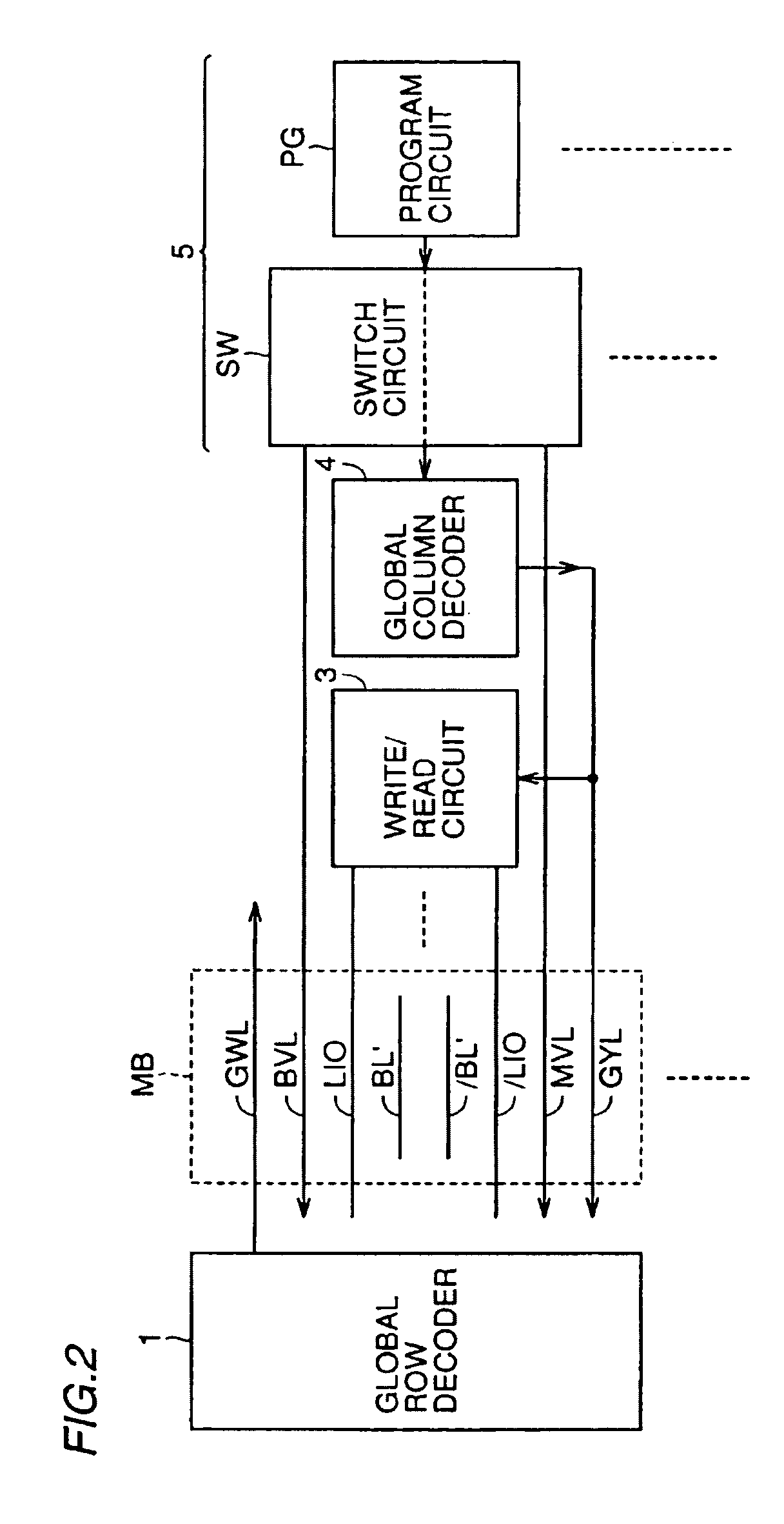
[0044]FIG. 1 is a diagram showing layout of an SRAM according to one embodiment of the present invention. In FIG. 1, the SRAM includes a global row decoder 1, a memory array region 2, a write / read circuit 3, a global column decoder 4 and a power supply control circuit 5 arranged in order in the X direction in the figure.

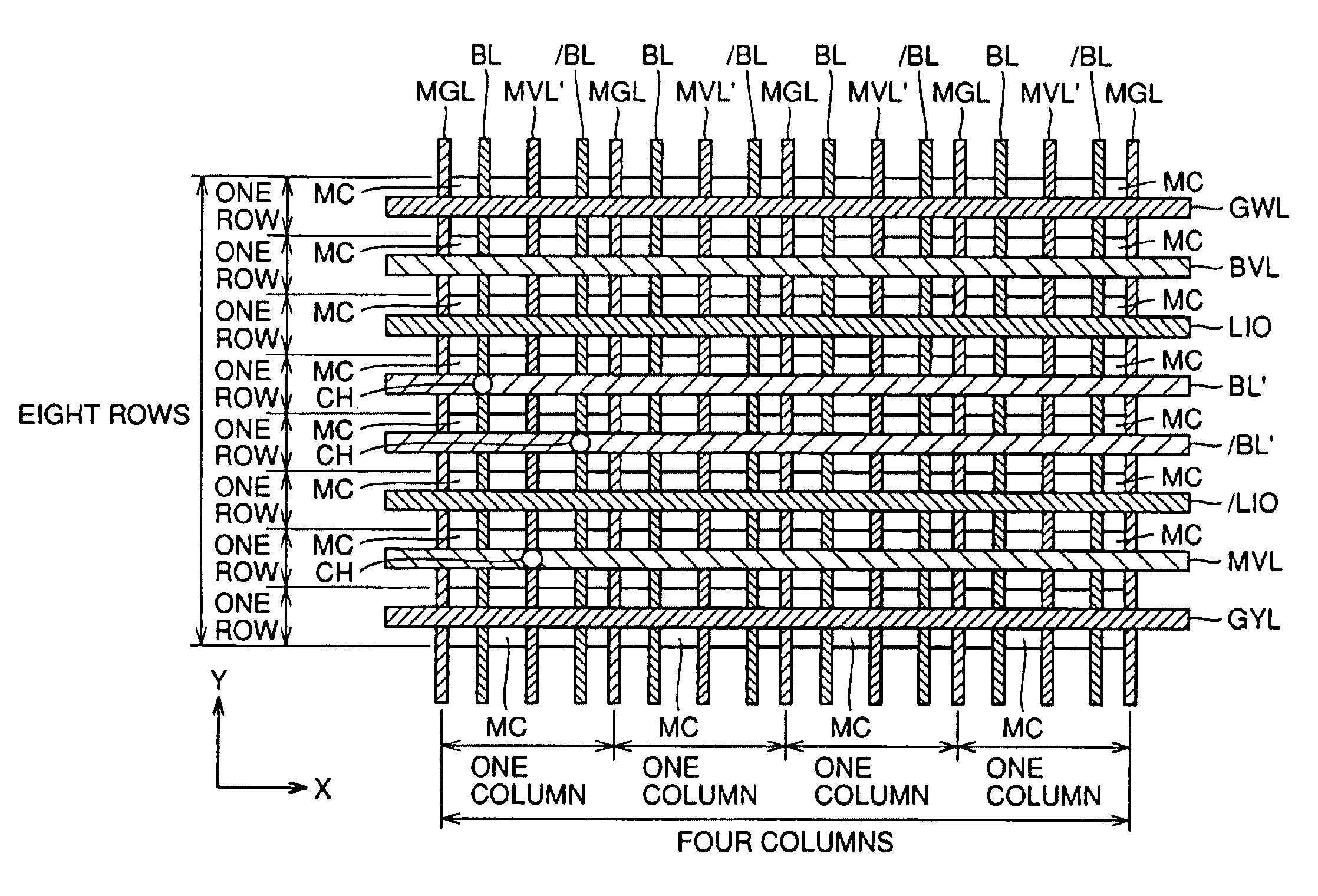
[0045]The memory array region 2 is divided into 2048 memory blocks MB arranged in 256 rows by 8 columns. Each memory block MB includes memory cells in 8 rows by 256 columns. In the memory array region 2, 4M bits of data can be stored. In each memory block MB column, two spare columns and 16 spare rows are provided.

[0046]In each memory block MB row, as illustrated in FIG. 2, a global word line GWL, a bit line load power supply line BVL, a local data input / output line pair LIO, / LIO, a memory cell power supply line MVL and a global column selecting line GYL are provided.

[0047]The global row decoder 1 selects one of the 256 global word lines GWL in response to a row add...


PUM


Abstract

Above a memory block including horizontal memory cells in 8 rows by 256 columns, a total of eight lines, a global word line, a bit line load power supply line, a local data input / output line pair, a bit line signal input / output line pair, a memory cell power supply line and a global column selecting line are, arranged at equal intervals. Since provision of one line is enough per one memory cell row, an SRAM having a T-type bit line structure can be realized with ease using horizontal memory cells to enable reduction of a layout area and speed-up of an operation rate.

Description

BACKGROUND OF THE INVENTION[0001]1. Field of the Invention[0002]The present invention relates to a static semiconductor memory device and, more particularly, to a static semiconductor memory device having a T-type bit line structure.[0003]2. Description of the Related Art[0004]Among conventional static random access memories (hereinafter referred to as SRAM), the mainstream is a memory cell of a high resistance and load type or a TFT load type having four transistors and two loads because it requires a small memory cell layout area. These memory cells, however, have lost their popularities as a power supply voltage of an SRAM has been decreased from 3 V to 2.5 V, 1.8 V and down to 1.5 V because they are not excellent in low-voltage operation characteristics, while a full CMOS cell having six transistors excellent in low-voltage operation characteristics is gaining a popularity.[0005]FIG. 13A is a circuit diagram showing a structure of such a full CMOS memory cell MC. In FIG. 13A, th...

Claims


Application Information

Patent Timeline
Patent Type & Authority Patents(United States)
IPC IPC(8): G11C5/06G11C11/41G11C11/413G11C11/418G11C11/419G11C29/04H01L21/8244H01L27/11
CPCG11C11/419G11C11/418
Inventor OHBAYASHI, SHIGEKI
Owner RENESAS TECH CORP
Why Eureka
Try Eureka