Solid-state image pickup device with non-hydrogen-absorbing waveguide

a solid-state image and waveguide technology, applied in the direction of radio frequency controlled devices, instruments, television systems, etc., can solve the problems of unavoidable formation of al film with poor adhesion relative to the surface of the insulating film, increased thickness of the insulating layer, and increased reflection, etc., to achieve satisfactory adhesion, satisfactory surface condition, and satisfactory coverage

Inactive Publication Date: 2006-05-09
SONY CORP
View PDF4 Cites 30 Cited by
  • Summary
  • Abstract
  • Description
  • Claims
  • Application Information

AI Technical Summary

Benefits of technology

[0055]According to the solid-state image pickup device of the present invention, since the waveguide is formed in the insulating layer on the light-receiving sensor portion, the side wall of the waveguide is covered with the reflective film made of the Al film formed by a CVD method, the underlayer film is formed between the reflective film and the waveguide and the underlayer film is made of the VIb-group element on the periodic table, hydrogen supplied to the light-receiving sensor portion when the solid-state image pickup device is manufactured can be prevented from being absorbed by the underlayer film.
[0056]Also, since the reflective film made of the Al film deposited by the CVD method can be deposited in the low temperature region, it is possible to obtain the waveguide including the reflective film with satisf

Problems solved by technology

However, as the insulating layer progressively increases its thickness in accordance with reduction of a size of a pixel and increase of multilayer interconnection layers, it is unavoidable that the increase of the thickness of the insulating layer will exert a more serious influence upon efficiency at which incident light is focused on the light-receiving sensor portion.
However, when the Al film is deposited by the CVD method, the following problems arise.
Thus, even when the Al film is deposited on the surface of the insulating layer, the coverage is lowered, the reflectivity is lowered by remarkably-uneven portions produced on the film surface, and further an Al film with poor adhesion relative to the surface of the insulating film is formed unavoidably.
Accordingly, the grain size of this continuous film is la

Method used


Image

  • Solid-state image pickup device with non-hydrogen-absorbing waveguide
  • Solid-state image pickup device with non-hydrogen-absorbing waveguide
  • Solid-state image pickup device with non-hydrogen-absorbing waveguide

Examples


Embodiment Construction

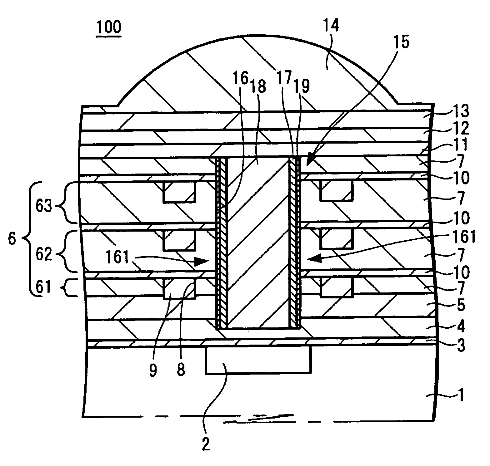
[0063]A solid-state image pickup device according to an embodiment of the present invention will now be described with reference to the drawings. FIG. 3 shows a schematic arrangement of a solid-state image pickup device in which the present invention is applied to a CMOS type solid-state image pickup device (CMOS sensor).

[0064]More specifically, FIG. 3 is a cross-sectional view showing one pixel portion of a CMOS type solid-state image pickup device according to an embodiment of the present invention.

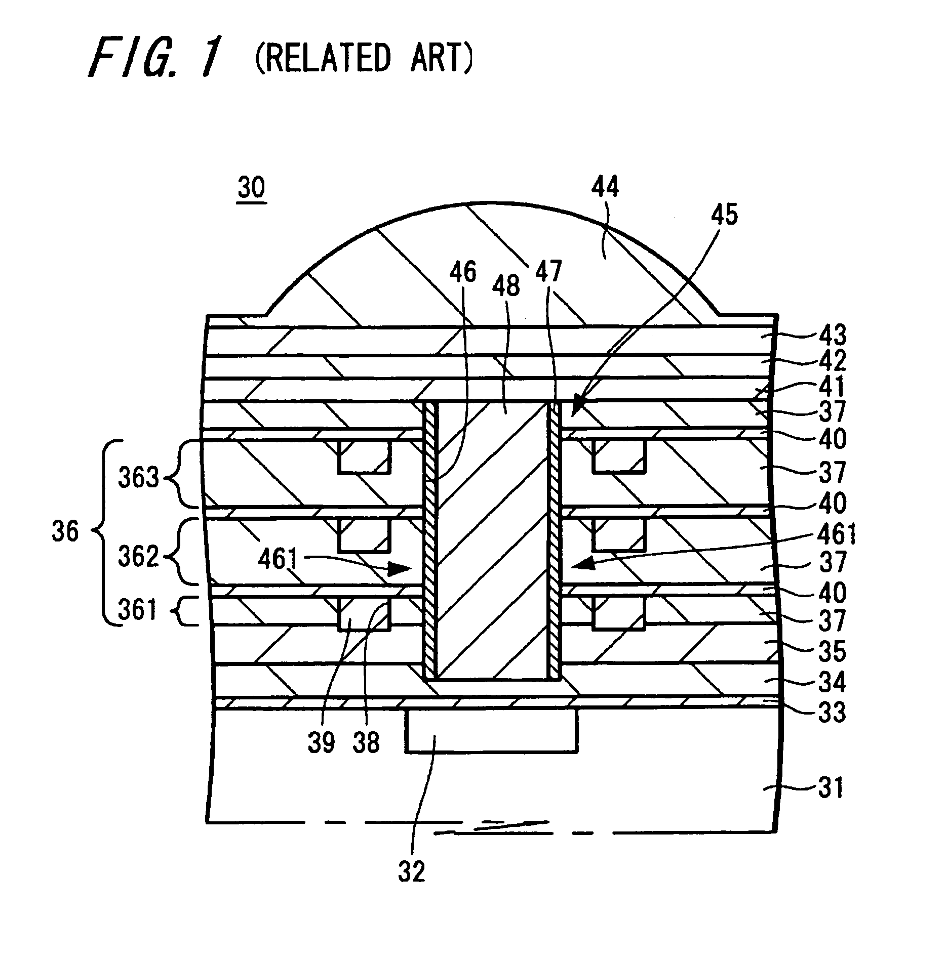
[0065]A CMOS type solid-state image pickup device, generally depicted by the reference numeral 100 in FIG. 3, includes a semiconductor substrate 1. A light-receiving sensor portion 2 is formed within the semiconductor substrate 1 at its predetermined position, and silicon oxide film (SiO film) 3, for example, having insulating function, surface protection function or surface planarization function is formed on the semiconductor substrate 1. The silicon oxide film 3 has formed thereon a ...


PUM


Abstract

A solid-state image pickup device 100 is constructed in which a waveguide 15 is formed in an insulating layer on a light-receiving sensor portion 2, a side wall 161 of the waveguide 15 is covered with a reflective film 17 made of an Al film deposited by a CVD method, an underlayer film 19 is formed between the reflective film 17 and the side wall 161 of the waveguide 15 and the underlayer film 19 is made of a VIb-group element. It is possible to obtain a solid-state image pickup device including a waveguide in which hydrogen supplied to the light-receiving sensor portion 2 can be restrained from being absorbed by the underlayer film 19 and which has the reflective film 17 of high reflectivity with satisfactory surface condition, satisfactory coverage and excellent adhesion.

Description

BACKGROUND OF THE INVENTION[0001]1. Field of the Invention[0002]The present invention relates to a solid-state image pickup device, and particularly to a solid-state image pickup device in which a light-receiving sensor portion has a waveguide provided thereon to increase efficiency at which incident light is focused on the light-receiving sensor portion.[0003]2. Description of the Related Art[0004]In most cases of a CCD (charge-coupled device) or a CMOS (complementary metal-oxide-semiconductor) type solid-state image pickup devices, it has an arrangement in which an on-chip microlens is disposed on a plurality of light-receiving sensor portions composed of photo-diodes, for example, comprising pixels through an insulating layer to bring a focal point of incident light passed through the on-chip microlens near the light-receiving sensor portion to thereby guide light into the light-receiving sensor portion.[0005]However, as the insulating layer progressively increases its thickness ...

Claims


Application Information

Patent Timeline
IPC IPC(8): H01L27/00H01L27/146H01L27/14H01L31/00H01L31/0232H04N5/225
CPCH01L27/14623H01L27/14625H01L27/14656H01L27/14636H01L27/14629H01L27/146H01L27/14
Inventor TAKAHASHI, SHINGOENOMOTO, YOSHIYUKIABE, HIDESHI
Owner SONY CORP
Why Eureka
Try Eureka