Method for producing micromechanic sensors and sensors produced by said method

a micromechanical sensor and manufacturing method technology, applied in the direction of fluid pressure measurement, fluid pressure measurement by electric/magnetic elements, instruments, etc., to achieve the effect of reliable production, sufficient mobility of silicon atoms on the substrate, and simple manufacturing method of micromechanical sensors

Inactive Publication Date: 2006-05-16
ROBERT BOSCH GMBH
View PDF16 Cites 18 Cited by
  • Summary
  • Abstract
  • Description
  • Claims
  • Application Information

AI Technical Summary

Benefits of technology

[0003]The method of the present invention has the advantage over the background art, that a particularly simple method for manufacturing micromechanical sensors is specified. In this context, the micromechanical sensors constitute sensor elements, which are made of monocrystalline silicon. The method is also suitable for the integration of circuit elements.
[0004]In order to ensure that a void is reliably produced, the introduced openings should be deeper than the diameter. They should preferably have a diameter of less than 1 μm and be deeper than 2 μm. Sufficiently high temperatures ensure that the mobility of the silicon atoms on the substrate is sufficient. The actual sensor elements are then formed by further processing steps. In this context, the deposition of an epitaxy layer and the introduction of dopants are advantageous.

Problems solved by technology

However, these structures are only intended to be used in integrated circuits.

Method used


Image

  • Method for producing micromechanic sensors and sensors produced by said method
  • Method for producing micromechanic sensors and sensors produced by said method
  • Method for producing micromechanic sensors and sensors produced by said method

Examples


Embodiment Construction

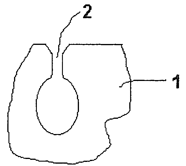
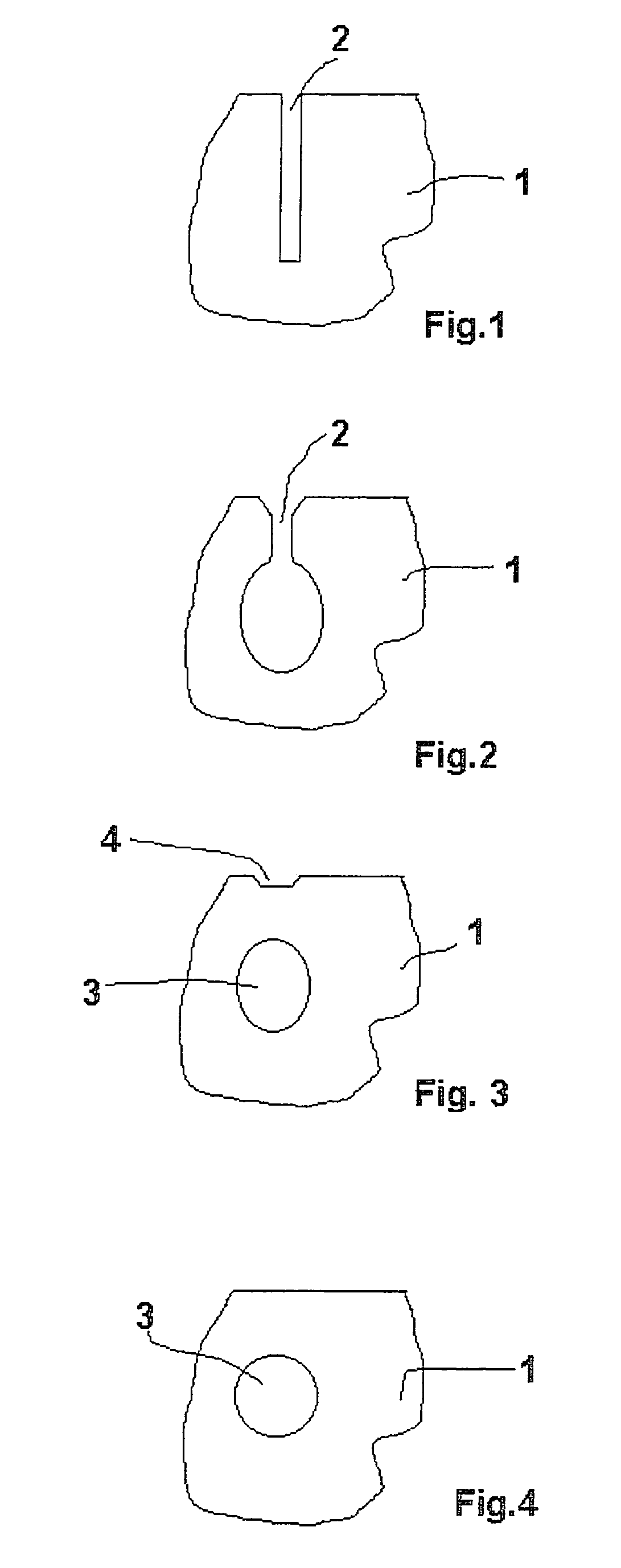
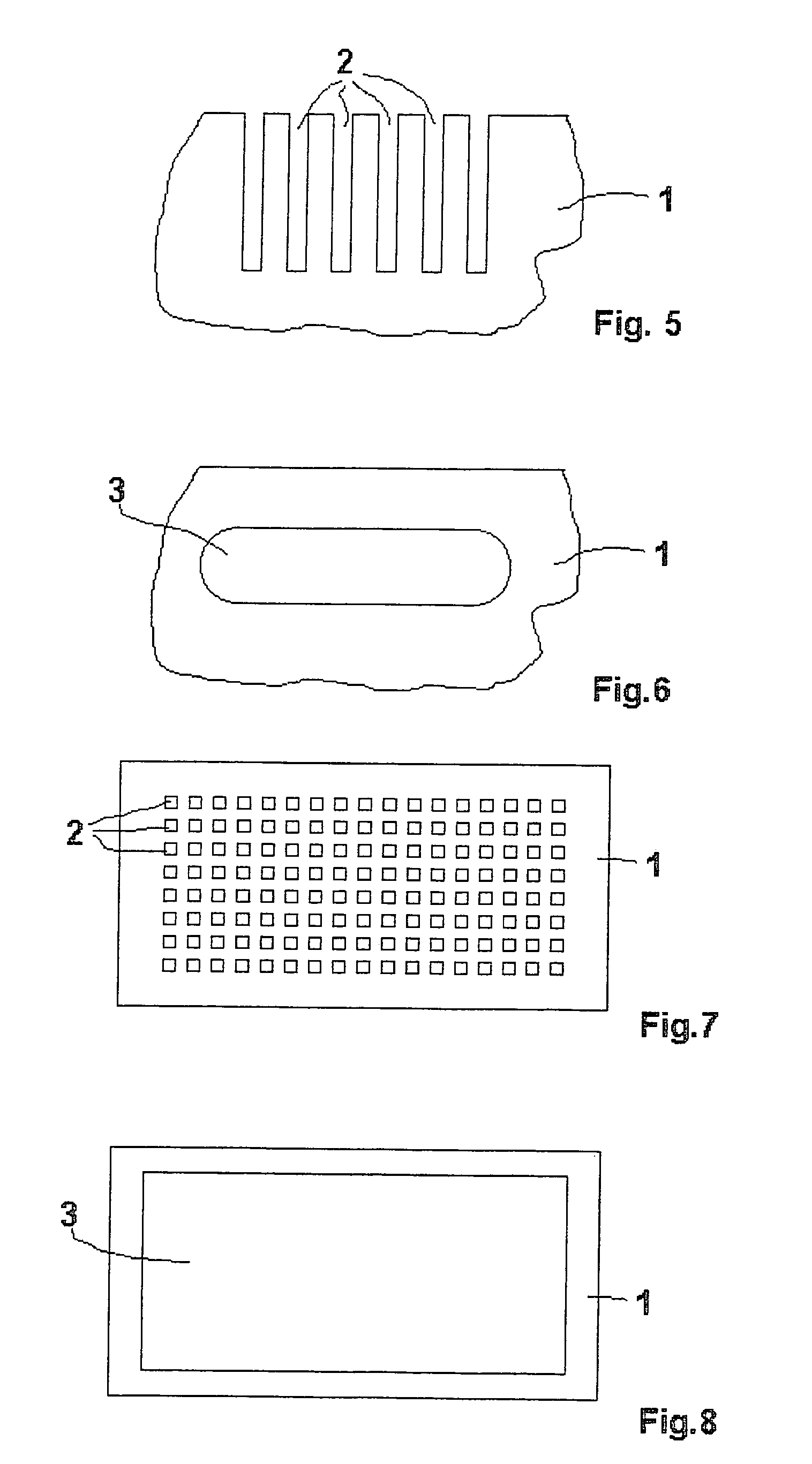
[0011]A process sequence elucidating the method of the present invention is shown in FIGS. 1 through 4. Shown in FIG. 1 is a cross-section of a silicon substrate 1, into which an opening 2 is introduced. Opening 2 takes the form of a long, thin, blind hole, which typically has a diameter of less than 1 μm and extends more than 1 μm into the depth of silicon substrate 1. Silicon substrate 1 is, in particular, a monocrystalline silicon substrate. Such openings may be produced by reactive ion etching, i.e. irradiating the surface of silicon substrate 1 with ions of a gas, which form a gaseous chemical compound with the silicon material. Usually, the part of the surface of silicon substrate 1 that should not be etched is protected by a masking of, for example, silicon oxide, silicon nitride, metals, or glass layers. A purely ablative, plasma-etching method may also be used as an alternative.

[0012]Silicon substrate 1, whose cross-section in shown in FIG. 1, is then subjected to a tempera...


PUM

PropertyMeasurementUnit
temperatureaaaaaaaaaa
depthaaaaaaaaaa

Abstract

Proposed is a method for manufacturing micromechanical sensors and sensors manufactured by this method, where openings are introduced into a semiconductor substrate. After the openings are introduced into the semiconductor substrate, a subsequent temperature treatment is carried out, in which the openings are converted into voids in the depth of the substrate.

Description

FIELD OF THE INVENTION[0001]The present invention relates to a method for manufacturing micromechanical sensors and micromechanical sensors produced by it.BACKGROUND INFORMATION[0002]An article of Mizushima et al., Applied Physics Letter, Vol. 77, No. 20, Nov. 13th, 2000, page 3290 ff., already describes a method, in which voids are produced in the semiconductor substrate by introducing openings and carrying out a subsequent temperature treatment. However, these structures are only intended to be used in integrated circuits. A multitude of other manufacturing processes, in particular the so-called sacrificial-layer technique, are known for manufacturing sensors. In this context, a silicon layer is produced on a sacrificial layer. The sacrificial layer is then removed again after the silicon layer is patterned.SUMMARY OF THE INVENTION[0003]The method of the present invention has the advantage over the background art, that a particularly simple method for manufacturing micromechanical...

Claims


Application Information

Patent Timeline
Patent Type & Authority Patents(United States)
IPC IPC(8): H01L21/00G01L9/00B81B3/00B81C1/00H01L29/84
CPCB81C1/00047B81C1/00246G01L9/0045G01L9/0042G01L9/0055B81B2203/033B81C2203/0742B81C2201/0116
Inventor BENZEL, HUBERTWEBER, HERIBERTARTMANN, HANSSCHAEFER, FRANK
Owner ROBERT BOSCH GMBH
Why Eureka
Try Eureka