Method of separating a release layer from a substrate comprising hydrogen diffusion

a technology of hydrogen diffusion and release layer, which is applied in the direction of electrical equipment, semiconductor devices, instruments, etc., can solve the problems of difficult mass production of tft, difficult growth of glass substrate and quartz substrate, and fragile and heavyness

Inactive Publication Date: 2006-05-16
SEMICON ENERGY LAB CO LTD
View PDF51 Cites 104 Cited by
  • Summary
  • Abstract
  • Description
  • Claims
  • Application Information

AI Technical Summary

Benefits of technology

[0009]In view of the foregoing, it is an object of the present invention to provide a separation method for easy separation of an allover release layer with a large area. A further object of the present invention is to provide the separating method that is not subjected to restrictions in the use of substrates, such as a kind of substrate, during forming a release layer.

Problems solved by technology

In such a display apparatus, a glass substrate and a quartz substrate are generally used, however, they have disadvantages such as being fragile and heavy.
In addition, the glass substrate and the quartz substrate are difficult to grow in size for mass-production.
However, in case of using a high performance polysilicon film for the active layer of a TFT, a high temperature process at several hundreds degrees is required for a manufacturing process, so that a TFT cannot be directly formed on a plastic film.
However, the above-described method requires a substrate that is very transparent to light, and comparative large amount of laser light irradiation for energizing enough to release hydrogen contained in amorphous silicon, so that a problem becomes arisen that a release layer is damaged.
In addition, according to the above described method, in case of forming a device over a separation layer and carrying out heat treatment or the like at high temperature during a manufacturing process, there is a threat that separation is inadequately carried out even if a laser light is emitted to a separation layer since hydrogen contained in the separation layer is decreased due to the heat treatment.

Method used


Image

  • Method of separating a release layer from a substrate comprising hydrogen diffusion
  • Method of separating a release layer from a substrate comprising hydrogen diffusion
  • Method of separating a release layer from a substrate comprising hydrogen diffusion

Examples


example 1

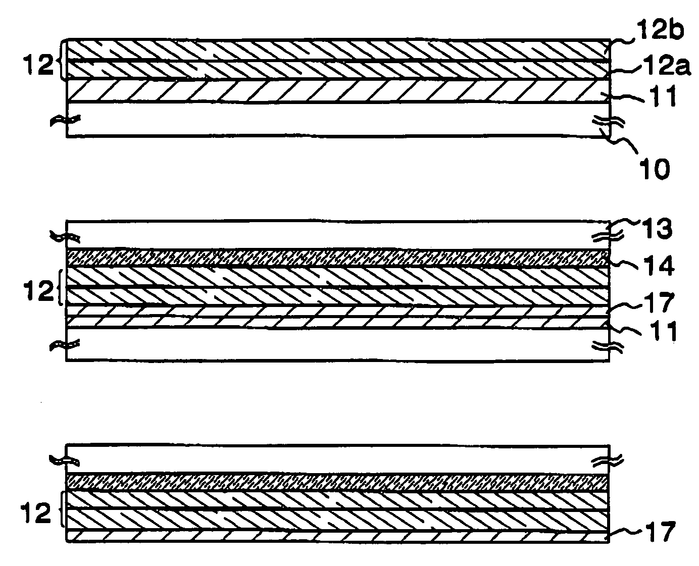
[0056]As shown in above described embodiment, the experiment that is demonstrated the fact that thin films are deposited sequentially, and oxide formed at a surface boundary between the metal film and the oxide film are reduced by heat treatment at 400° C. or more, then, the film containing the oxide or a surface boundary between the film and another film is split will be explained hereinafter. In the following experiment, a tungsten film is used as the metal film, a silicon oxide film as the oxide film included in the release layer, and an amorphous silicon film is used as the semiconductor film.

experiment 1

[0057]AN 100 glass substrate (126×126 mm) as a substrate, a tungsten (W) film (50 nm) deposited by sputtering as a metal film, a silicon oxide film (200 nm) deposited by sputtering as a protective film, a silicon oxynitride (SiON) film (100 nm) deposited by CVD as a base film, and an amorphous silicon film (54 nm) deposited by CVD as a semiconductor film are sequentially formed. Thereafter, samples 1 to 6, each of which are heat treated for 1 hour at 500° C., 450° C., 425° C., 410° C., 400° C., and 350° C., and a sample 7, which is heat treated for 1 hour at 350° C. in the hydrogen atmosphere are prepared. Then, separation experiments are respectively carried out to the samples 1 to 7 using a polytetrafluoroethylene tape. FIGS. 4A to 4G are photographs of the experiments.

[0058]As shown in FIGS. 4A to 4G, samples 1 to 4, which are heat treated at 410° C. or more can be separated, however, samples 5 and 6 cannot be separated, that is, a semiconductor film or the like does not adhere t...

experiment 2

[0061]As in the case with the experiment 1, AN 100 glass substrate (126×126 mm) as a substrate, a tungsten film (50 nm) deposited by sputtering as a metal film, a silicon oxide film (200 nm) deposited by sputtering as a protective film, a silicon oxynitride (SiON) film (100 nm) deposited by CVD as a base film, and an amorphous silicon film (54 nm) deposited by CVD as a semiconductor film are sequentially formed. A sample A that is not heat treated, a sample B that is heat treated for 1 hour at 220° C., and a sample C that is heat treated for 1 hour at 500° C., and further, for 4 hours at 550° C. are prepared and TEM analysis is carried out. FIGS. 5A, 5B, and 6A are each TEM image, and FIG. 6B is a view showing the frame format of each of the TEM image.

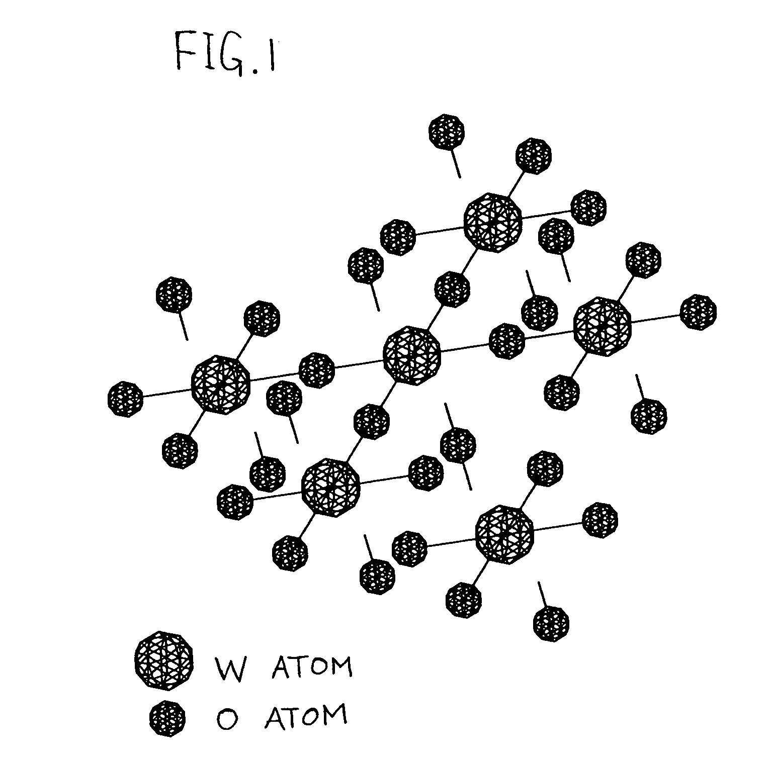
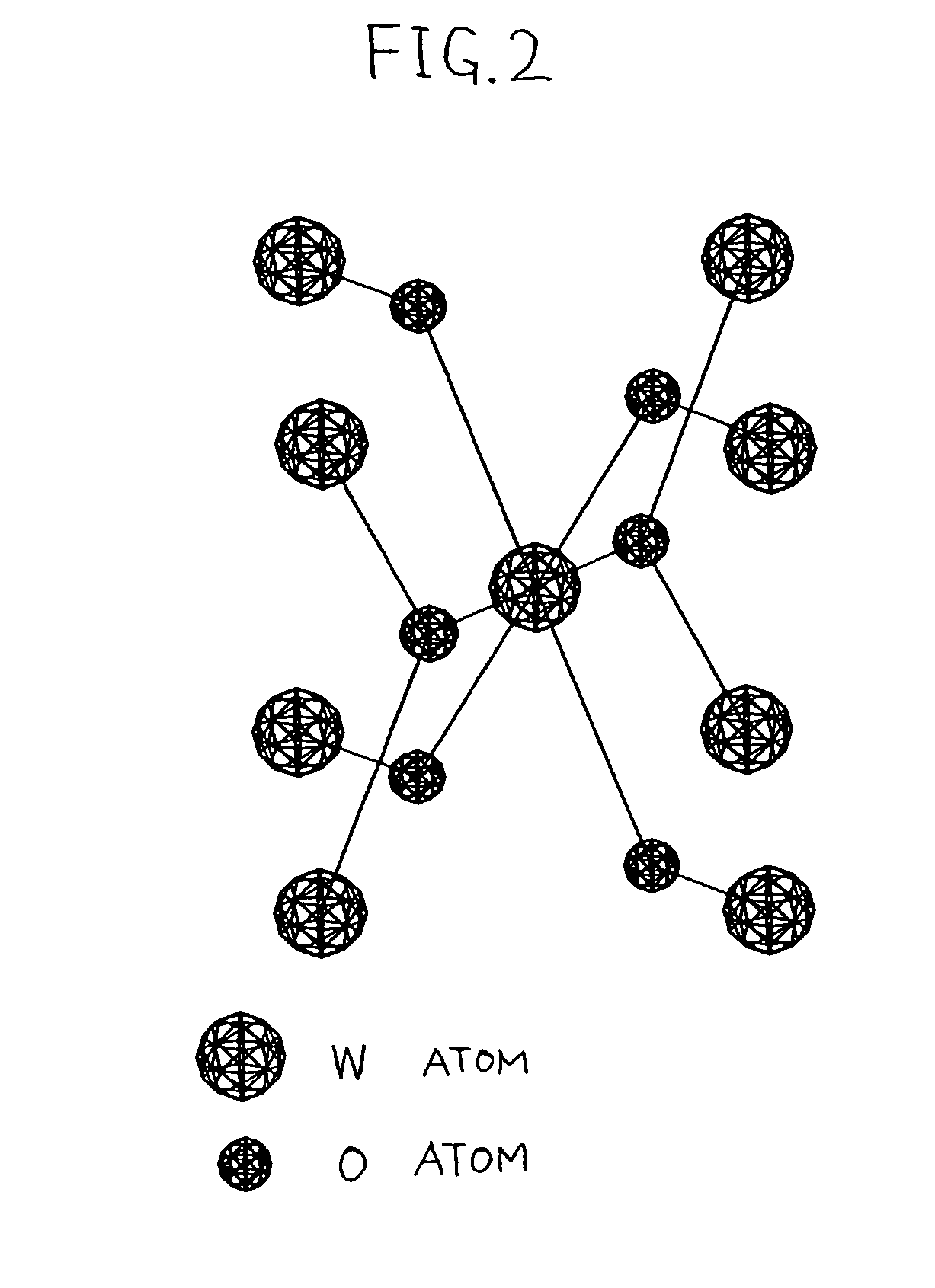
[0062]As shown in all TEM images, a new film (hereinafter, unknown film) is formed at a surface boundary between the tungsten film and the silicon oxide film. Compared with TEM images each other, only the unknown film of the sample C h...


PUM

PropertyMeasurementUnit
temperatureaaaaaaaaaa
thicknessaaaaaaaaaa
thicknessaaaaaaaaaa

Abstract

The present invention is a separation method for easy separation of an allover release layer with a large area. Further, the present invention is the separating method that is not subjected to restrictions in the use of substrates, such as a kind of substrate, during forming a release layer. A separation method comprising the steps of forming a metal film, a first oxide, and a semiconductor film containing hydrogen in this order; and bonding a support to a release layer containing the first oxide and the semiconductor film and separating the release layer bonded to the support from a substrate provided with the metal layer by a physical means. Through the separation method, heat treatment is carried out to diffuse hydrogen contained in the semiconductor film, a third oxide is formed by reducing a second oxide formed at a surface boundary between the metal film and the first oxide film, and a film containing the second oxide and the third oxide, a surface boundary between the film containing the second oxide and the third oxide, and the metal film, or a surface boundary between the film containing the second oxide and the third oxide, and the first oxide is split.

Description

BACKGROUND OF THE INVENTION[0001]1. Field of the Invention[0002]The present invention relates to a method for separating a release layer. Specifically, the present invention relates to a method for separating a release layer including various devices. And more specifically, the present invention relates to an electric appliance including a display apparatus as typified by a liquid crystal module, an EL (electroluminescent) module, or the like, as one of components.[0003]2. Related Art[0004]In recent years, a technique for forming a TFT composed of a semiconductor thin film (with a thickness of approximately from several to several hundreds nm) formed over an insulating surface of a substrate has attracted attention. TFTs are used for an electric device such as IC, an electro-optic device, or the like, and are especially developed as a switching device or a driver circuit of a display apparatus.[0005]In such a display apparatus, a glass substrate and a quartz substrate are generally ...

Claims


Application Information

Patent Timeline
Patent Type & Authority Patents(United States)
IPC IPC(8): H01L21/46H01L21/30H01L29/786G02F1/136H01L21/00H01L21/68H01L21/77
CPCH01L21/6835H01L27/1214H01L27/1266H01L2924/3025H01L2221/68359H01L2221/68368H01L29/786
Inventor MARUYAMA, JUNYAOHNO, YUMIKOTAKAYAMA, TORUGOTO, YUUGOYAMAZAKI, SHUNPEI
Owner SEMICON ENERGY LAB CO LTD
Why Eureka
Try Eureka