Frequency measuring device, polishing device using the same and eddy current sensor

a technology of eddy current sensor and measuring device, which is applied in the direction of semiconductor/solid-state device testing/measurement, lapping machine, instruments, etc., can solve the problems of abandoning the entire semiconductor substrate, increasing manufacturing costs, and producing semiconductor wafers that cannot be used, etc., and achieves short time intervals and high precision.

Inactive Publication Date: 2006-05-16
SCI MED LIFE SYST +1
View PDF15 Cites 34 Cited by
  • Summary
  • Abstract
  • Description
  • Claims
  • Application Information

AI Technical Summary

Benefits of technology

[0035]The present invention has been proposed to solve the problems in the frequency measurement of the above-described conventional eddy current sensor, and, therefore, an object of the present invention is to provide a frequency measuring device and method capable of obtaining a frequency measurement result with high precision and in a short time interval, and a polishing device and method using the same.
[0036]Further, the present invention has an object to provide an eddy current sensor capable of operating stably and detecting an end point of the polishing accurately.
[0063]Since the frequency measuring device according to the present invention has the above-mentioned structure, the present invention can provide the frequency measured result of the measured signal every given time interval at which an arbitrary length can be set, thereby resulting in such an advantage that the measured result can be obtained every period shorter than that in the conventional frequency measuring device. In addition, an outstanding effect of increasing significant digits of the measured frequency can be obtained. Therefore, by applying such a frequency measuring device to the polishing device, a precision with which the end point of polishing of the semiconductor wafer is detected can be remarkably improved.
[0067]As described above, since the oscillator circuit is integrally formed of the sensor coil forming part of the eddy current sensor, and the active element unit connected to the sensor coil, the coaxial cable can communicate signals at a low impedance (50 Ω), and the oscillator circuit can be stably operated without picking up noise caused by rotation of the turn table and the like of an associated polishing apparatus. Also, the substrate including the active element unit is disposed in a direction perpendicular to the sensor coil, so that an eddy current loss can be detected using a high oscillating frequency in the VHF band. It is therefore possible to detect an eddy current loss in a thin conductive film having a high resistivity and to detect a polishing state of a thin film on the order of angstroms such as a tantalum (Ta) film or the like which is used as a barrier layer. For this reason, a polishing end point can be detected in a significantly high accuracy.
[0068]According to a seventh aspect of the present invention, there is provided an eddy current sensor for detecting the thickness of a conductive film from a change in an eddy current loss generated in the conductive film, comprising a sensor coil for generating an eddy current in the conductive film, wherein a change in the thickness of the conductive film is detected from a change in a resistance component in an impedance formed by the sensor coil and the conductive film. Since this eddy current sensor detects a change in the thickness of a conductive film associated with the advancement of polishing by observing a change in a resistive component with the oscillating frequency left fixed, it is possible to clearly observe a polishing state of an extremely thin film at a relatively low frequency. Thus, the eddy current sensor has the ability to readily detect the thickness of an extremely thin barrier layer which has a low conductivity.

Problems solved by technology

In this way, in the CMP process, when the unnecessary electrically conductive film on the semiconductor wafer is removed, if the conductive film is over-polished, a conductor for forming a wiring circuit is also removed, which results in a semiconductor wafer being produced that cannot be used.
Also, since an insufficient polishing of the electrically conductive film cannot remove the conductive films that short-circuit between the wiring circuits, it is necessary to further continue polishing, thereby resulting in an increase in the manufacturing cost.
In this event, if the Cu layer is excessively polished to remove the Cu layer in the grooves for wiring together with the oxide film (SiO2), a resulting increase in circuit resistance would lead to the abandonment of the entire semiconductor substrate, thereby sustaining a great damage.
On the other hand, the Cu layer remaining on the oxide film due to insufficient polishing would fail to separate wiring circuits, thereby resulting in short-circuiting.
Consequently, the polishing process must be performed again, thereby causing an increase in manufacturing cost.
However, as the eddy current loss exists, a resistance component in the oscillator circuit is increased due to the influence of an equivalent resistance component of a semiconductor wafer, thereby causing the oscillating frequency to move toward a higher region.
The conventional method of detecting a polishing end point based on the eddy current sensor, however, suffers from the following problems.
The removal of the noise is difficult in the course of output signal processing in the oscillator circuit.
Further, the oscillating frequency used for the eddy current sensor is relatively low, i.e., approximately 7 MHz so that a large eddy current loss can be detected when a conductive film subjected to polishing has a sufficient thickness, whereas when the eddy current loss becomes smaller as the conductive film is polished more so that its thickness becomes extremely smaller, in which case difficulties are encountered in detecting, for example, a thickness of approximately 1000 Å or less.
In other words, because of a relatively low oscillating frequency utilized for detection, the conventional eddy current sensor fails to provide a sufficiently high accuracy for detecting an end point for polishing performed by a polishing apparatus which requires a thickness detection accuracy on the order of angstroms.

Method used


Image

  • Frequency measuring device, polishing device using the same and eddy current sensor
  • Frequency measuring device, polishing device using the same and eddy current sensor
  • Frequency measuring device, polishing device using the same and eddy current sensor

Examples


Embodiment Construction

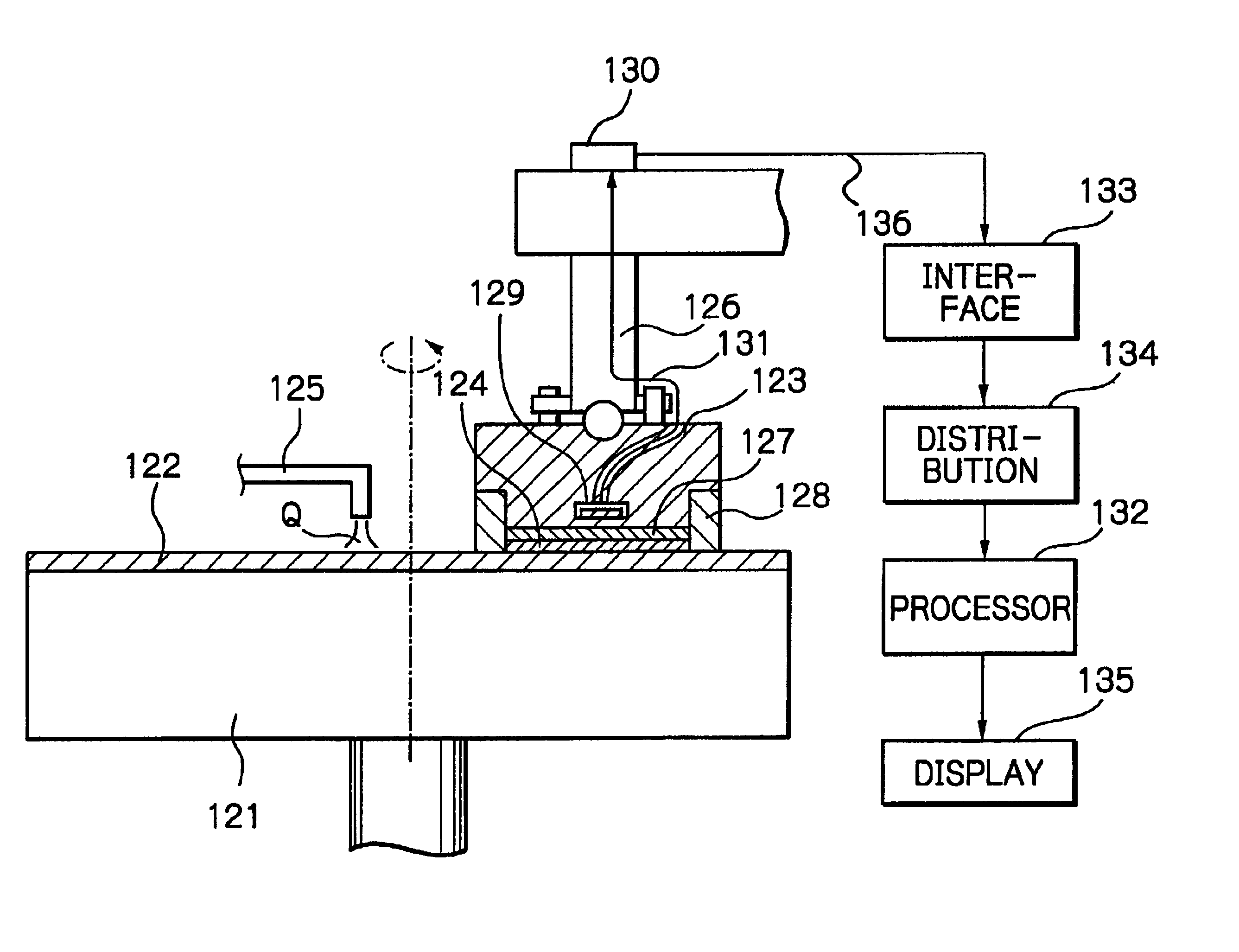
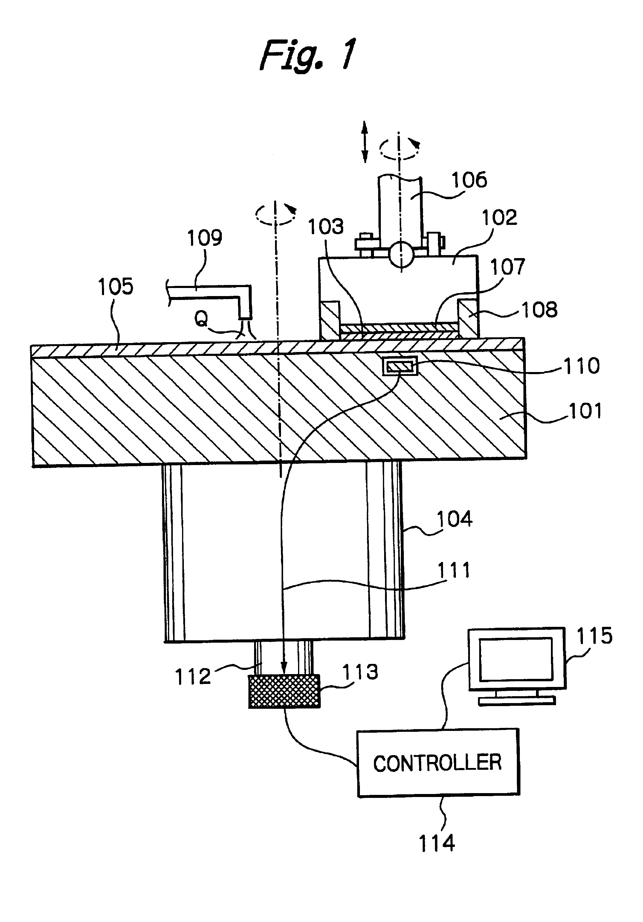
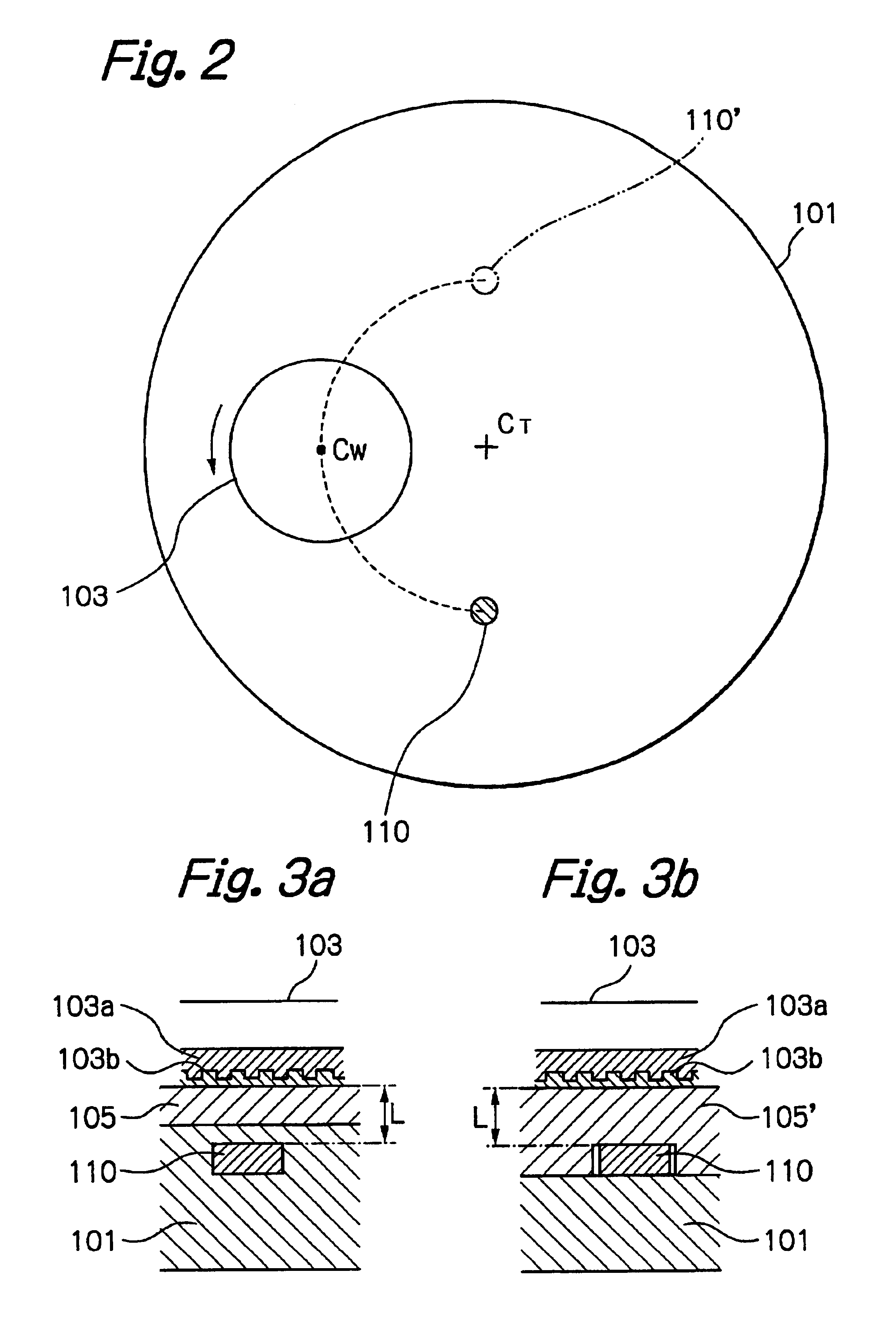
[0093]Now, a description will be given of preferred embodiments of a frequency measuring device using a sequential counting system, according to the present invention as described herein. First, referring to FIG. 7, a frequency measuring device FC includes i decimal counters 1, 2, 3, 4, . . . i, in which i is an integer of 2 or more. The input terminals of these decimal counters 1-i are connected to the output terminals of respective corresponding gate circuits G1-Gi, and also the outputs of the decimal counters 1-i are connected to the input terminal of a latch circuit 11 in parallel. The latch circuit 11 supplies a value latched by the latch circuit 11 to a desired processing circuit through an I / O port 12 at given intervals.

[0094]A measured signal Vin having a pulse waveform is supplied to an input terminal IN of an amplifier A, and the measured signal Vin amplified by the amplifier A is supplied to one input terminal of each of the gate circuits G1-Gi in parallel. The other inpu...


PUM

PropertyMeasurementUnit
resonance frequencyaaaaaaaaaa
oscillating frequencyaaaaaaaaaa

Abstract

A frequency measuring device capable of accurately detecting an end point of polishing a semiconductor wafer by obtaining a frequency measurement result highly accurately in a short period of time. A device FC, which measures the frequency of a measured signal comprises a counting section including a plurality of n-nary counters, a time reference circuit which outputs a time reference signal for every predetermined time interval, and a plurality of gate circuits whose outputs are connected to the inputs of the n-nary counters. The gate circuits receive the measured signal at a first input and receive the time reference signal at the predetermined time intervals at a second input. With this structure, the counting section supplies the frequency measured result of the measured signal every predetermined time interval.

Description

BACKGROUND OF THE INVENTION[0001]The present invention relates to a frequency measuring device capable of measuring a frequency highly accurately and continuously within a short period and to a device and method for polishing by using the frequency measuring device.[0002]Further, the present invention relates generally to an eddy current sensor, and more particularly, to an eddy current sensor which is capable of detecting an eddy current loss produced in a conductive film made of copper (Cu) or the like deposited on the surface of a substrate such as a semiconductor wafer, when the conductive film is polished by a chemical mechanical polishing (CMP) technique, to detect the advancement of polishing, and a method of detecting a polished thickness using the eddy current sensor.[0003]A chemical mechanical polishing (CMP) process has been widely employed as a method in which a semiconductor substrate is dipped in a plating solution to conduct, for example, electrolytic plating or non-e...

Claims


Application Information

Patent Timeline
Patent Type & Authority Patents(United States)
IPC IPC(8): G01B7/06H01L21/304B24B37/013B24B49/04B24B49/10G01D5/20G01N27/72G01R23/10G01R33/12
CPCB24B37/013B24B49/04B24B49/10G01R23/10G01B7/105G01D5/202B24B49/105H01L21/304
Inventor TADA, MITSUOYAMASAKI, HIRONOBUSUTO, YASUNARI
Owner SCI MED LIFE SYST
Why Eureka
Try Eureka