Solid state imaging apparatus and method for driving the same

a technology of solid-state imaging and imaging apparatus, which is applied in the direction of radiological control devices, instruments, television systems, etc., can solve the problems of long charge time, difficult to achieve a small-sized solid-state imaging device, and inability to obtain high-quality images. , to achieve the effect of low cos

Inactive Publication Date: 2006-05-16
SONY CORP
View PDF18 Cites 10 Cited by
  • Summary
  • Abstract
  • Description
  • Claims
  • Application Information

AI Technical Summary

Benefits of technology

[0036]In this method of driving a solid state imaging apparatus according to the present invention, two pixel lines are selected by the vertical selection means and signals output from the respective pixels in the selected two pixel lines are independently read by the signal processing means thereby obtaining pixel signals the amplitudes of which depend linearly on the amount of light incident on the solid state imaging apparatus during two respective periods without encountering a signal overflow from the photoelectric conversion element which can occur in the techniques disclosed in the previous patent applications, and thus obtaining an image signal with a large dynamic range from the pixel signals.
[0037]This method according to the present invention can be implemented without needing an additional special circuit. Thus, the method makes it possible to take a high-accuracy image with a large dynamic range under various imaging conditions and makes it possible to realize a high-performance, small-sized and low-cost solid state imaging apparatus.

Problems solved by technology

The offset component varies from one pixel 120 to another, and such variation in offset component can cause noise.
However, in this solid state imaging device, it takes a long time to charge or discharge a capacitor, which can result in an afterimage.
Another problem is that the structure of this solid state imaging device does not allow use of an embedded photodiode (in which, the photodiode is formed below, for example, a p+-layer covered with an insulating film at the top) having an advantage of low noise, and thus a high-quality image cannot be obtained.
A still another problem is that a large number of circuit elements are needed and thus it is difficult to achieve a small-sized solid state imaging device.
However, this technique needs a line memory or a frame memory, which results in increases in device size and cost.
Another problem is that because two pictures taken at different times are mixed together, it is difficult to obtain a picture of a moving subject.
However, in this technique, calculation associated with adjacent lines is needed, and thus the device becomes complicated in structure and large in size.
Besides, mixing of two pictures into a single picture results in a reduction in resolution.
However, in the techniques disclosed in the previous patent applications, a signal with a large dynamic range is generated only when light incident on a photodiode (PD) is so high in intensity that an overflow of a charge occurs, and thus the signal does not vary linearly depending on the amount of light in a low-intensity range.
This makes it difficult to precisely calculate the intensity of light from the normal signal and the signal with the large dynamic range.
Therefore, those techniques are not suitable for applications such as machine vision or measuring instruments in which determination of the precise amount of light is needed, although the techniques can be used in monitor cameras or the like without encountering significant problems.
When the techniques are applied to color pictures, the inaccuracy in the intensity of light results in inaccuracy in color, that is, the resultant color becomes unnatural.

Method used


Image

  • Solid state imaging apparatus and method for driving the same
  • Solid state imaging apparatus and method for driving the same
  • Solid state imaging apparatus and method for driving the same

Examples


second embodiment

[0082]Now, the present invention is described below.

first embodiment

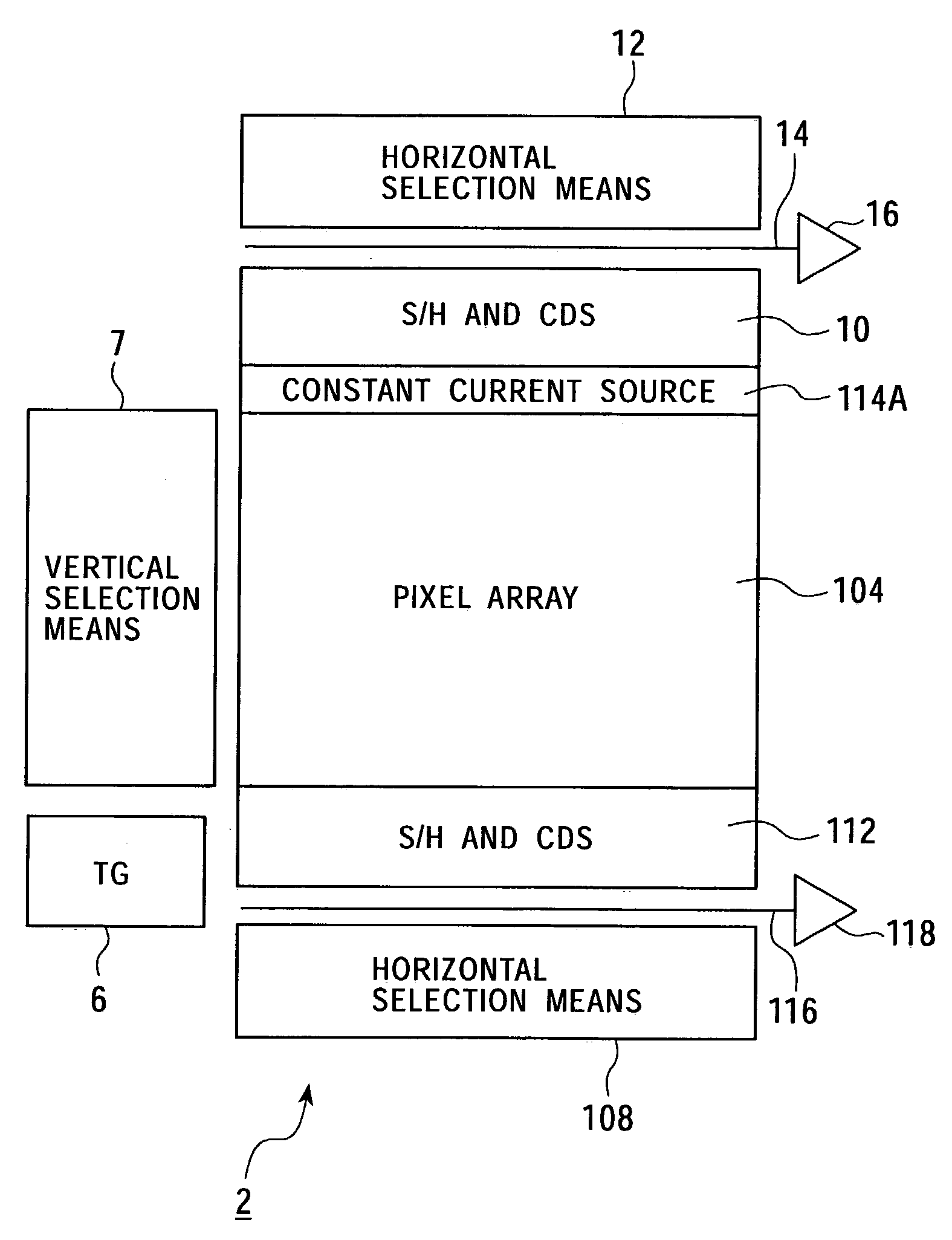
[0083]In the present invention described above, pixel signals in the second shutter line are output (as the output 1) from the output unit 118, and pixel signals in the selection line are output (as the output 2) from the output unit 16, and thus the signals output from the output units 118 and 16 originate from different lines. This makes it necessary to delay one of the output signals using a delay element or a memory before the two output signals are mixed together to obtain a final signal with a large dynamic range.

[0084]In the second embodiment described below, to avoid the above problem, two signals are output from the same pixel at the same time thereby making it possible to directly mix the two signals without using a delay element or a memory.

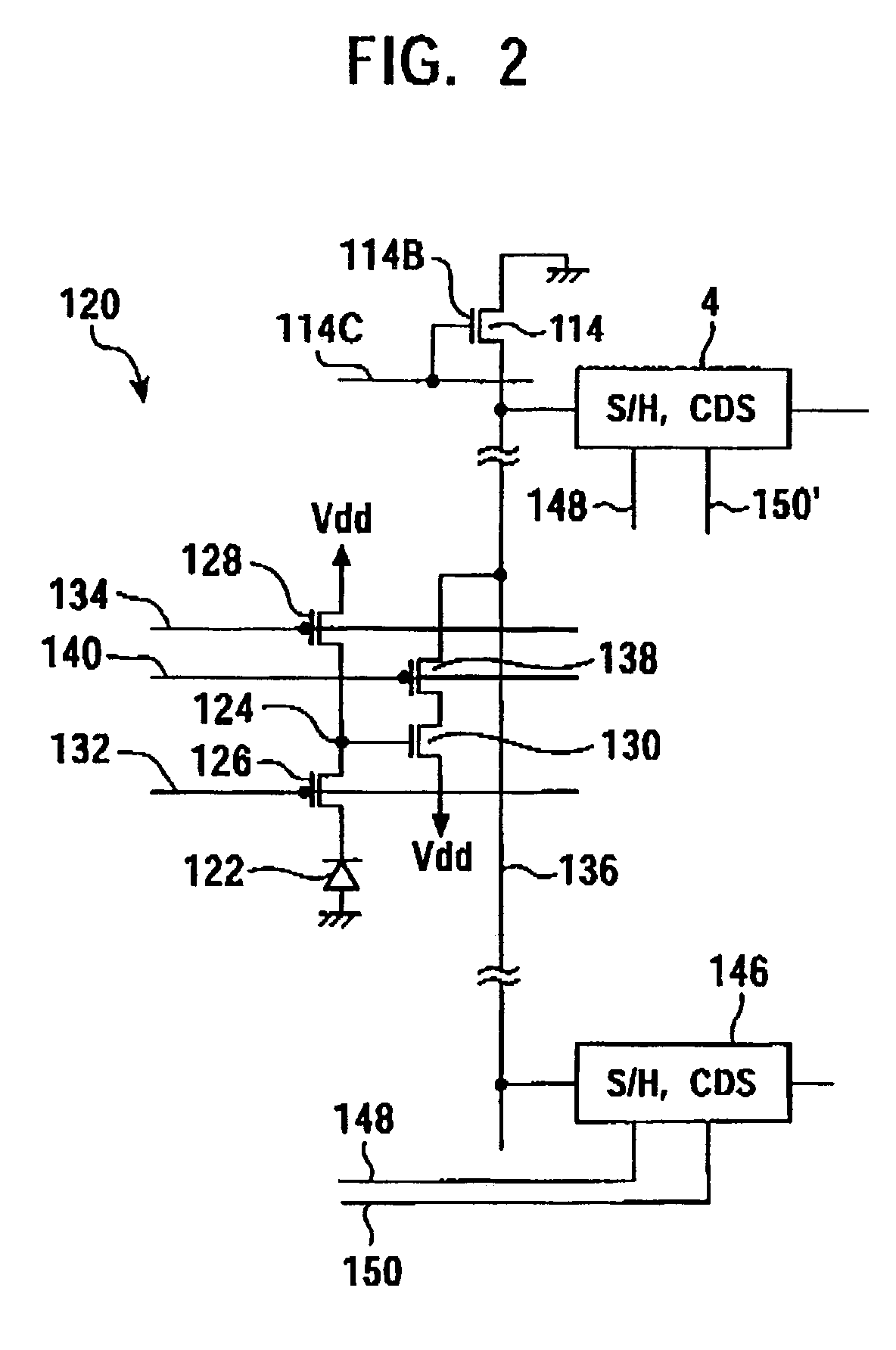
[0085]The solid state imaging apparatus according to this second embodiment of the invention can be constructed in the same manner as shown in FIG. 1, and each pixel can be constructed in the same manner as shown in FIG. 2. Furthermore...

third embodiment

[0113]the present invention is described below.

[0114]FIG. 6 shows a solid state imaging apparatus according to the third embodiment of the present invention.

[0115]As shown in FIG. 6, the solid state imaging apparatus 34 according to the present embodiment includes a communication unit 54 for receiving an external signal for controlling the driving mode of the solid state imaging apparatus 34.

[0116]In FIG. 6, the horizontal selection means 108 and the horizontal selection means 12 are combined together into a single horizontal selection means 168, and the S / H-CDS circuits 146 and 4 and the output units 118 and 16 are combined into CDS-AGC units 160 and 162. The output signals from the CDS-AGC circuits 160 and 162 are mixed together by a signal mixer-A / D converter 164, and the resultant mixed signal is output in the form of a digital signal over a bus line 166. Essentially, these circuit elements are similar to those of the solid state imaging apparatus 3 shown in FIG. 1, and they are...


PUM


Abstract

The vertical selection circuit of the imaging apparatus selects a selection line, a first shutter line, and a second shutter line to divide a single frame into three parts at arbitrary ratios. A first output signal is generated during a period from the first shutter line to the second shutter line and a second output signal generated during a period from the second shutter line to the selection line. By mixing the two output signals described above, an image with a large dynamic range can be obtained.

Description

[0001]This application claims priority to Japanese Patent Application No. JP2001-392170 filed Dec. 25, 2001, which is incorporated herein by reference.BACKGROUND OF THE INVENTION[0002]1. Field of the Invention[0003]The present invention relates to a solid state imaging apparatus and a method for driving a solid state imaging apparatus, and more particularly, to a solid state imaging apparatus and a method for driving a solid state imaging apparatus, capable of detecting light over a large dynamic range.[0004]2. Description of the Related Art[0005]FIG. 9 shows a conventional solid state imaging apparatus, and FIG. 10 shows a pixel and its peripheral part of the solid state imaging apparatus shown in FIG. 9. FIG. 11 is a timing chart showing an operation of the circuit shown in FIG. 10.[0006]More specifically, the solid state imaging apparatus 102 shown in FIG. 9 is a CMOS photosensor made up of a pixel array 104 formed on a semiconductor substrate, vertical selection means 106, horiz...

Claims


Application Information

Patent Timeline
Patent Type & Authority Patents(United States)
IPC IPC(8): G09G5/00H04N5/335H01L27/146H04N5/341H04N5/353H04N5/355H04N5/369H04N5/374H04N5/376
CPCH04N5/2355H04N3/155H04N23/741H04N25/531H04N25/583H04N25/767H04N25/745
Inventor MABUCHI, KEIJI
Owner SONY CORP
Why Eureka
Try Eureka