Multi-pixel liquid crystal cell array

a liquid crystal cell array and multi-pixel technology, applied in static indicating devices, instruments, non-linear optics, etc., can solve the problems of low insertion loss, decreased optical performance, and inability to provide the same high performance of integrated structures, and achieve accurate control of cell gap thickness.

Inactive Publication Date: 2006-05-16
II VI DELAWARE INC
View PDF53 Cites 19 Cited by
  • Summary
  • Abstract
  • Description
  • Claims
  • Application Information

AI Technical Summary

Problems solved by technology

As a result, the performance of integrated structures usually do not offer the same level of high performance provided by the nanostructure alone.
It is generally known that the performance of liquid crystal technology is susceptible to temperature and humidity change, and that high humidity and temperature changes cause decreased optical performance, resulting in high insertion loss and low extinction, two critical measures of a cell's performance.
More specifically, changes in optical versus electrical response with atmosphere changes generally renders the prior art liquid crystal devices unstable and nonrepeatable.
Jackson does not accommodate feedback to the voltage control of the cell and fails to handle ambient temperature increases above the trip point.
McCartney's design, however, does not scale to high resolution optical systems without increasing the size of the lookup table.
These devices are generally affixed to the outside glass of the cell at disparate locations so they are generally incapable of functioning uniformly across the cell.
This can result in hysterises and other effects that distort the effectiveness of closed loop temperature sensing and heating systems.
Finally, prior-art liquid crystal cell heaters and temperature sensors are typically attached to the cell using epoxy resins, and epoxy resins are generally known to absorb moisture in high temperatures and high humidity conditions, which leads to degradation or inconsistency in cell performance.
The advantage of a seal of glass frit is known to be that such seal is practically impervious to gas and vapors, but this approach requires formation by high temperature processing, and high temperature processing tends to distort the substrate and render difficult control uniformity of the distance between the inner surface of the parallel substrates.
It is known that this second heating cycle tends to soften the substrates and cause warpage thereof, with the result that cells, particularly those of larger surface area, sealed by this glass frit method tend to have a very low percentage of acceptable manufacture.
However, such organic polymer sealants have a relatively high permeability to water vapor.
Under high temperature and humidity conditions, water vapor permeates into the seal causing the expansion of the seal and a shape change in the liquid crystal cavity that results in a change in the known performance of the liquid crystal cell

Method used


Image

  • Multi-pixel liquid crystal cell array
  • Multi-pixel liquid crystal cell array
  • Multi-pixel liquid crystal cell array

Examples


first embodiment

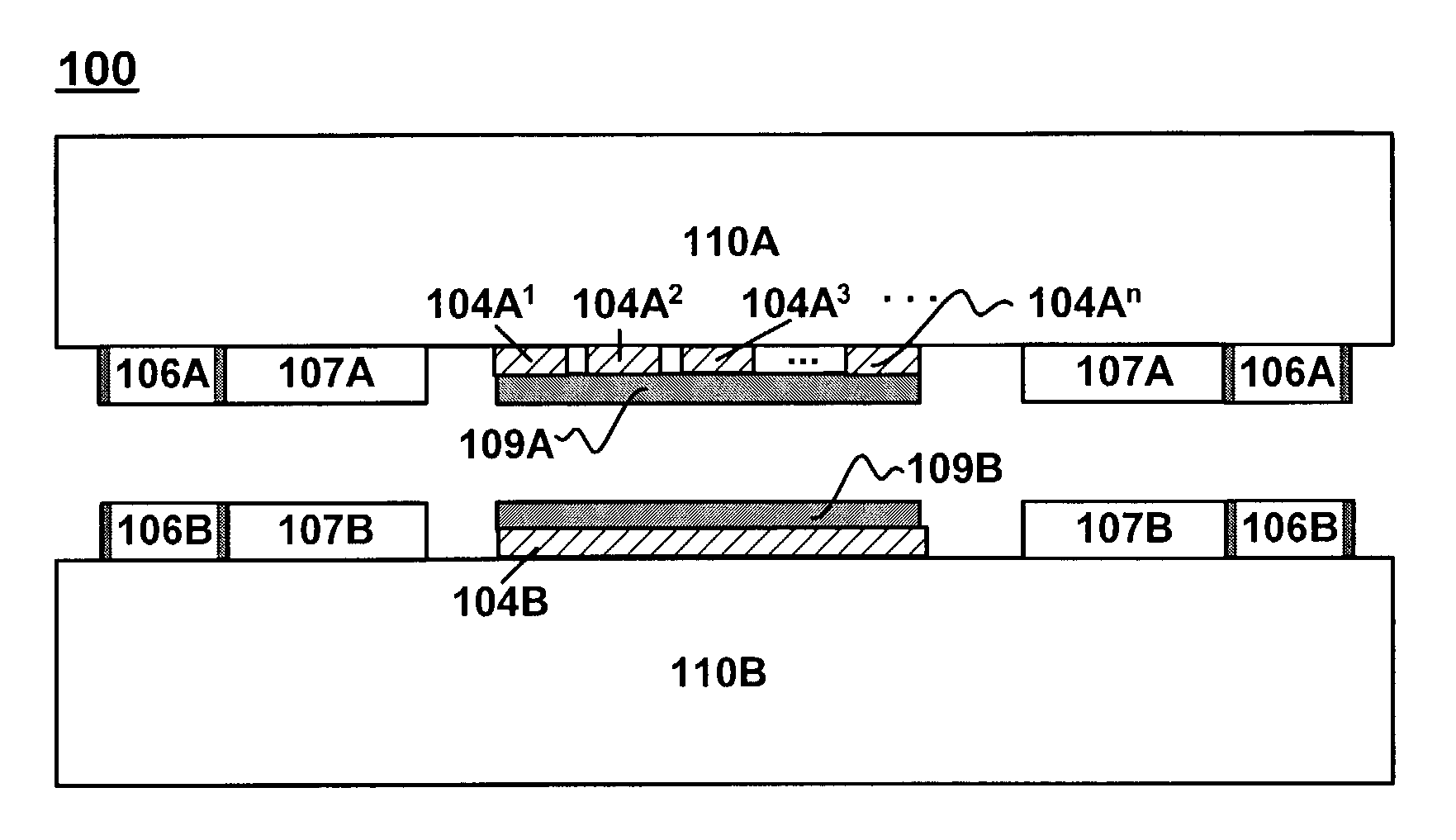
[0061]the present invention is presented in FIGS. 1a and 1b, which shows a multi-pixel liquid crystal cell platform 100 having a first substrate 110A in opposition to a second substrate 110B. In this embodiment, the first substrate may contain an inner surface having a conductive electrode layer 104 patterned to form individual pixel locations 104A1 through 104An, liquid crystal alignment layer 109A, a metal gasket element layer 106A and spacer element layer 107A. The second substrate 110B contains an inner surface having a common a conductive electrode layer 104B spanning the pixels defined above, a liquid crystal alignment layer 104B, metal gasket element layer 106B and spacer element layer 107B. In this embodiment and all embodiments, is preferred to maintain a common electrode 104B across multiple pixels in the array since it may form a ground plane common to the array. However, it need be noted that within the scope of this invention it will be clear that a multi-pixel mask sim...

second embodiment

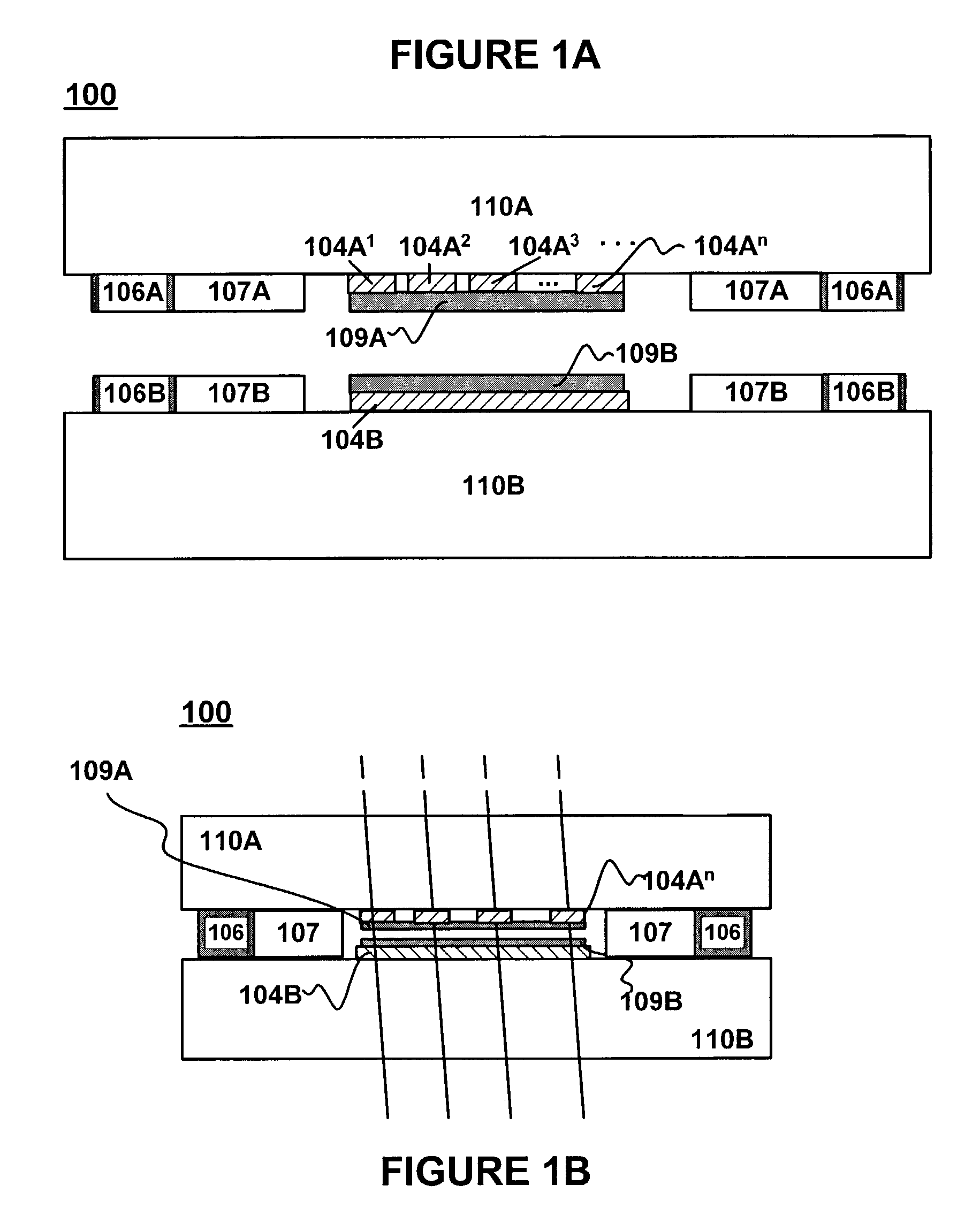
[0062]the present invention includes an integrated optical element 111 and is presented in FIGS. 2a and 2b, which shows a multi-pixel liquid crystal cell platform 100 having a first substrate 110A in opposition to a second substrate 110B wherein the first substrate contains a global integrated optical element 111 on one side of the substrate that performs an optical function across multiple pixel locations, a conductive electrode layer 104 patterned to form individual pixel locations 104A1 through 104An, a liquid crystal alignment layer 109A, metal gasket element layer 106A and spacer element layer 107A on the opposing side, and, the second substrate 110B containing a common conductive electrode layer 104B spanning the pixels defined above, a liquid crystal alignment layer 109B, metal gasket element layer 106B and a spacer element layer 107B.

[0063]A variation of the second embodiment of the present invention is presented in FIGS. 2c and 2d, which shows a multi-pixel liquid crystal c...

third embodiment

[0064]the present invention is presented in FIGS. 3a and 3b, which shows a multi-pixel liquid crystal cell platform 100 having a first substrate 110A in opposition to a second substrate 110B wherein the first substrate contains integrated optical elements 111n positioned at referential pixel locations, a conductive electrode layer 104 patterned to form individual pixel locations 104A1 through 104An, a liquid crystal alignment layer 109A, a metal gasket element layer 106A, and a spacer element layer 107A. In this embodiment, the second substrate 110B contains a common conductive electrode layer 104B spanning the pixels defined above, a liquid crystal alignment layer 104B, metal gasket element layer 106B, and a spacer element layer 107B.

[0065]A first variation of the third embodiment of the present invention is presented in FIGS. 3c and 3d, which shows a multi-pixel liquid crystal cell platform 100 having a first substrate 110A in opposition to a second substrate 110B wherein the firs...


PUM

PropertyMeasurementUnit
thickaaaaaaaaaa
rub anglesaaaaaaaaaa

Abstract

A multi-pixel optical processing system includes a multi-pixel liquid crystal cell platform having a deposited metal gasket moisture barrier bonding two opposing substrates each having a spacer layer to accurately control cell gap thickness. A library of specialized pixel constructs is included that can be configured to yield predetermined optical functions at referential locations in the platform. A control system is provided utilizing a time division scheme that multiplexes temperature sensing and heating functions across an optional integrated active thermal element that may be integrated inside the liquid crystal platform. A calibration process characterizes the profile of the cell and generates a polynomial regression formula that provides the voltage drive output for all pixels in the platform based on the platform temperature and state of each pixel.

Description

CROSS-REFERENCE TO RELATED APPLICATIONS[0001]This application is a continuation of and claims priority from commonly assigned application Ser. No. 10 / 371235, titled “Liquid Crystal Cell Platform”, filed Feb. 21, 2003. This application is also related to the following copending U.S. nonprovisional applications, all of which are herein incorporated by reference; “Fabrication Method for Liquid Crystal Cell”, filed Feb. 21, 2003 and having Ser. No. 10 / 371976, “Thermal Control System for Liquid Crystal Cell”, filed Feb. 21, 2003 and having Ser. No. 10 / 371983, and “Liquid Crystal Variable Optical Attenuator”, filed Mar. 3, 2003 and having Ser. No. 10 / 379384.FIELD OF INVENTION[0002]This invention relates generally to optical liquid crystal systems. More particularly, it relates to multi-pixel liquid crystal cell platforms.BACKGROUND OF THE INVENTION[0003]Since the advent of fiber optics, the fiber optical communication infrastructures have become more diverse and sophisticated. The fiber o...

Claims


Application Information

Patent Timeline
Patent Type & Authority Patents(United States)
IPC IPC(8): G02F1/1339G02FG02F1/09G02F1/13G02F1/133G02F1/1333G02F1/1335G02F1/1343G02F1/31
CPCG02F1/133382G02F1/133528G02F1/1339G02F1/31G02F1/093G02F1/1326G02F2203/12G02F2001/133521G02F2001/13355G02F2201/305G02F2203/055G02F2203/06G02F1/133521G02F1/13355
Inventor AUSTIN, LINDSAY W.CAVANAUGH, SHANTI A.MOLINARI, LOUIS J.YOUNG, MARK E.
Owner II VI DELAWARE INC
Why Eureka
Try Eureka