FET type sensor, ion density detecting method comprising this sensor, and base sequence detecting method

a sensor and ion density technology, applied in biochemistry apparatus and processes, instruments, transistors, etc., can solve the problems of unstable output in time, low sensitivity of isfet, and inability to detect ion density at high precision

Inactive Publication Date: 2006-05-23
BAIO TSUKUSU +1
View PDF11 Cites 236 Cited by
  • Summary
  • Abstract
  • Description
  • Claims
  • Application Information

AI Technical Summary

Benefits of technology

[0022]To solve the second problem (detection of hybridization), this invention is characterized by using a single-strand nucleic acid complementary to the specimen, as a substance to be fixed in the sensing section. Hence, without increasing the DNA by PCR method or the like, the presence of target nucleic acid in the sample can be detected simply, quickly and at low cost, so that the base sequence can be determined easily.
[0045]Further, this invention forms a plurality of the composite type sensors on a same semiconductor substrate, and detects a plurality of complementary nucleic acid structures in the specimen efficiently and simultaneously.
[0046]By using the ion sensor having such constitution, the invention opens a new dimension in the biochemical field, in particular, for judging the presence of specific organisms in samples or nucleic acid having a base sequence specific to disease, detecting presence or absence of organisms or diseases easily and securely, and content of organisms, and measuring endocrine-disrupting chemicals, dioxins and related substances.
[0061]For executing the above four methods, this invention comprises a pair of FET type sensors disposed on a same semiconductor substrate, an electrochemically inert outer peripheral wall enclosing the peripheral edges of the pair of FET type sensors in batch, and a partition wall partitioning between the sensors with the both ends internally contacting with the outer peripheral wall, wherein the sample solutions contained in each sensor do not communicate with each other, a target substance reacting with the specimen is fixed on the one sensor only, out of the two adjacent sensors on the same substrate, and nothing is fixed on the other sensor, and by using the same sample solution, the time-course drifts of solution or substance are measured by the other sensor, and the drift value is subtracted from the measured value of the one sensor, and thereby the compatibility of the specimen and target substance can be detected accurately.

Problems solved by technology

However, the ISFET is low in sensitivity (theoretical maximum sensitivity determined from Nernst equation is 59 mV / pH), and is unstable in output in terms of time, and ion density cannot be detected at high precision.
This method is, however, complicated in operation, and it takes much time and cost.

Method used


Image

  • FET type sensor, ion density detecting method comprising this sensor, and base sequence detecting method
  • FET type sensor, ion density detecting method comprising this sensor, and base sequence detecting method
  • FET type sensor, ion density detecting method comprising this sensor, and base sequence detecting method

Examples


embodiment 1

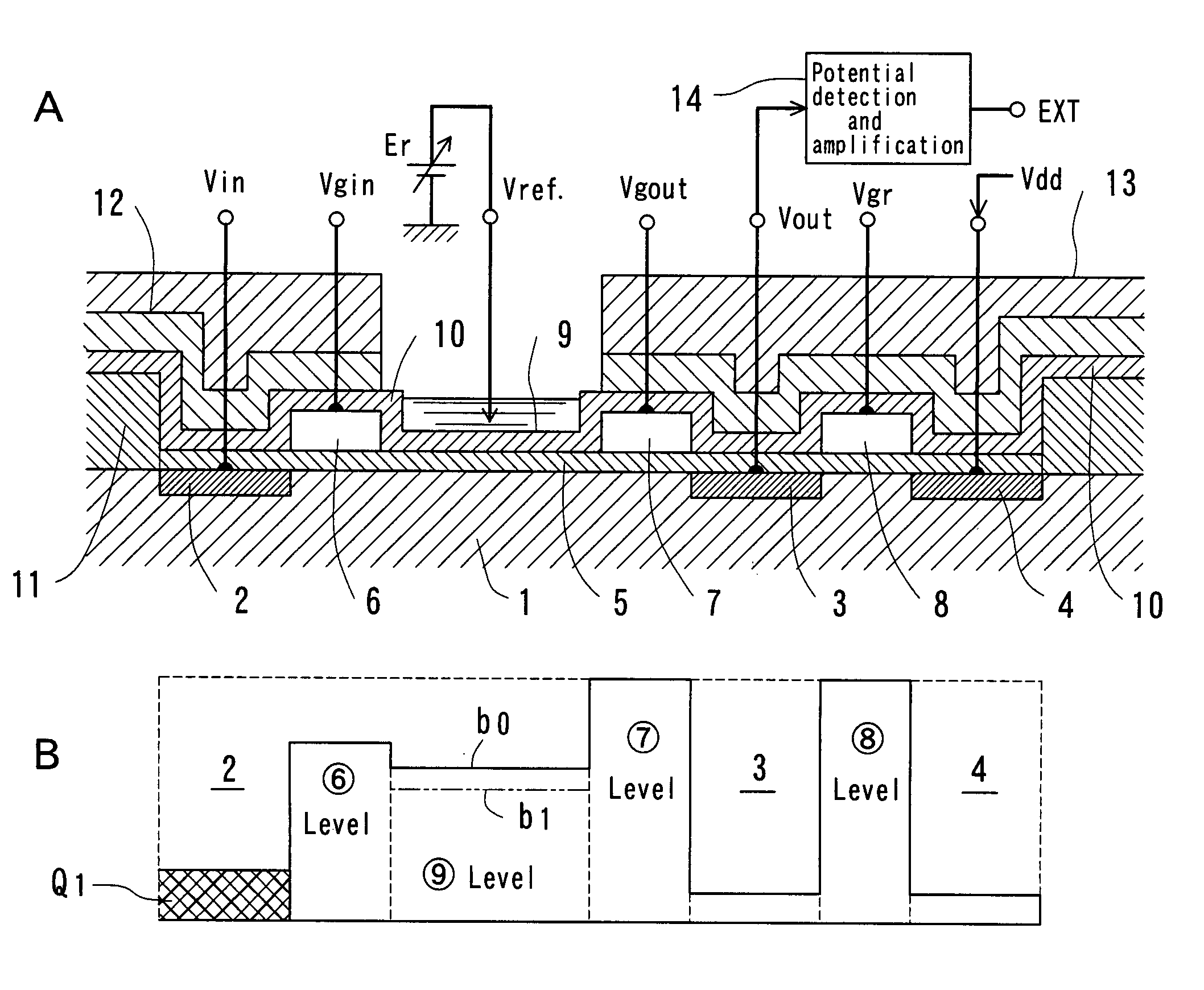
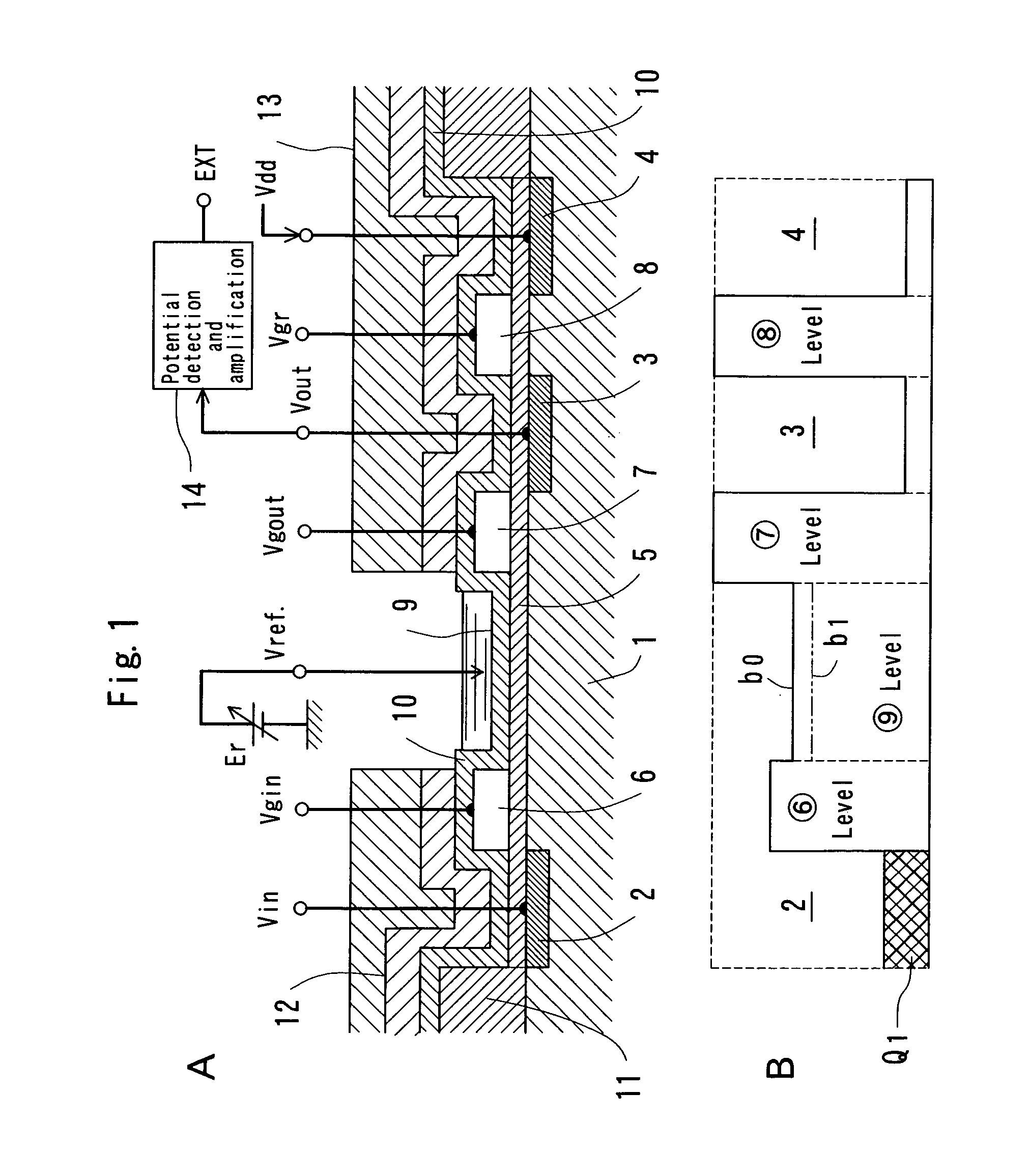
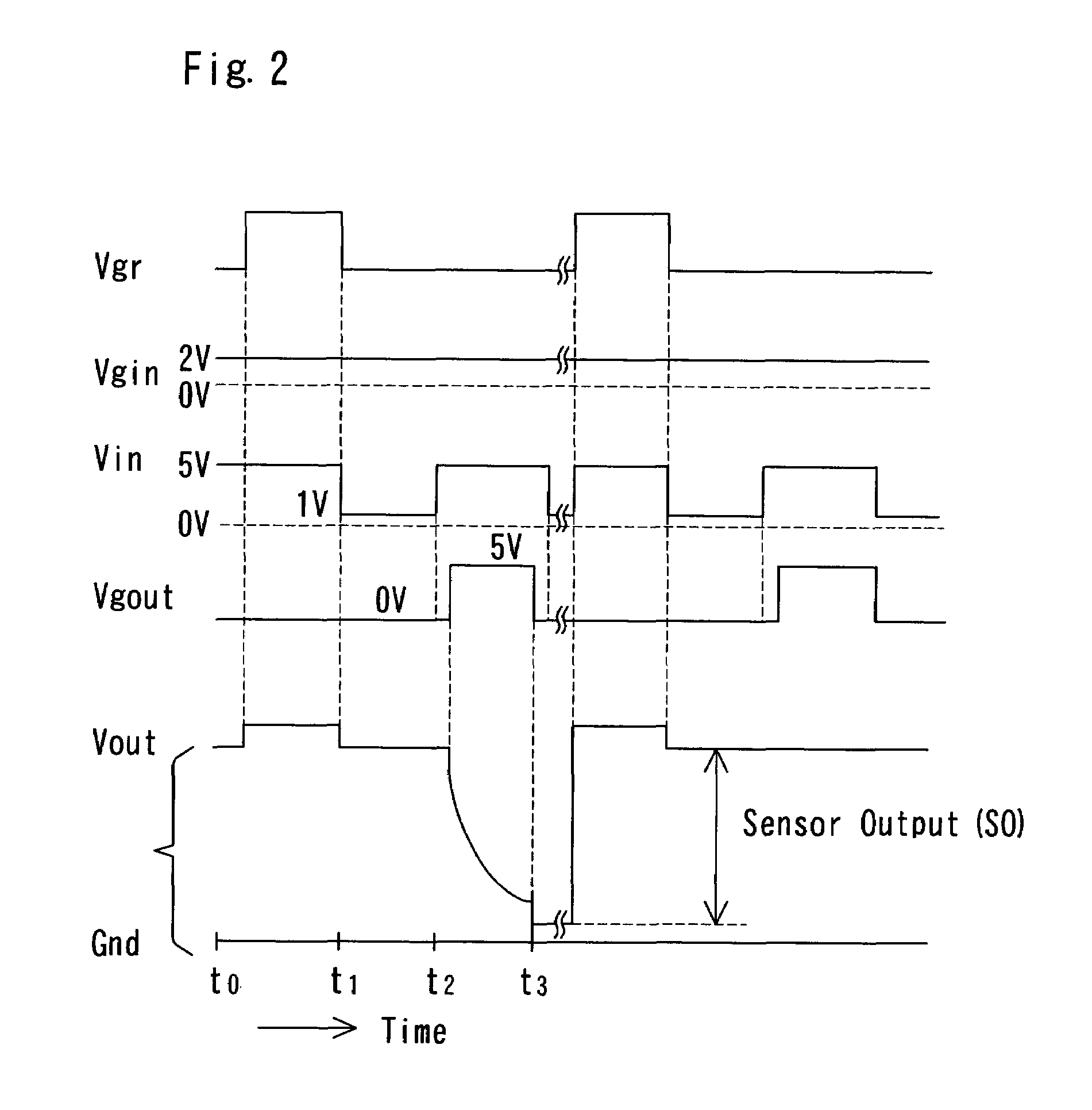
[0073]FIG. 1 is a sectional view (A) and a schematic view (B) showing a basic potential state of FET type sensor in Embodiment 1 of the invention, and FIG. 2 is a schematic view sequentially showing each potential state in the operating state. In FIG. 1A, reference numeral 1 is typically a p− type semiconductor substrate made Of silicon, and the face side of the semiconductor substrate 1 includes an input diode 2 and a floating diffusion section (FD) 3 as charge supply sections composed of n+ type diffusion layer formed across a specific interval, and a reset diode 4 is formed at a further small Interval from the floating diffusion section 3. On the semiconductor substrate 1, in this case, an insulation film 5 made of SiO2 or Si3N4 is formed, including on the n+ type diffusion layer.

[0074]On the surface of the semiconductor substrate 1 between the input diode 2 and floating diffusion section 3, a conductive channel (n type inversion layer) is formed in relation to the gate structure...

embodiment 2

[0092]FIG. 4 is a sectional view (A) and a schematic view (B) showing a basic potential state of FET type sensor in Embodiment 2 of the invention, and FIG. 5 is a schematic view showing the transition of potential state and accumulated charge. In the drawings, same parts as in FIG. 1 and FIG. 3 are identified with same reference numerals, and the explanation is simplified or omitted.

[0093]The FET type sensor in Embodiment 2 is similar to that in Embodiment 1, that is, at the surface side of a P− type semiconductor substrate, an input diode 2 and a floating diffusion section 3 comprising a diffusion region reverse to the substrate in conductivity, that is, N+ type are formed across a specific interval, and a reset diode 4 is also formed, and a reset gate 8 is formed on an insulation film 5 between the floating diffusion section 3 and reset diode 4, thereby forming a reset transistor for the floating diffusion section 3, and the structure above the insulation film 5 between the input ...

application example 1

[0122]In FIG. 7, a broken line circle 15 is a sample solution storing range surrounding the sensing section 9 or 9′ comprising an ion sensitive film formed on the surface insulation film of the semiconductor substrate, and the region of the substrate surface (insulation film) including at least its periphery. Those supposed to be included in this range 15, such as gate electrode (concealed beneath the insulation film), diode reverse to the substrate in conductivity type, and other diffusion layer (in this case, N+ layer), are represented by the floating diffusion section 3 relating to the sensor output shown in a broken line frame, and the relation with the sensor entire picture is suggested.

[0123]On the sensing section 9 or 9′ comprising an ion sensitive film such as Si3N4, a gold film (or a film of material having electrochemical stability and conductivity similar to the properties of gold film; same hereinafter) 16 is formed partly, and near the sensing section 9 or 9′ (at the le...


PUM

PropertyMeasurementUnit
reverse bias voltageaaaaaaaaaa
voltage Vginaaaaaaaaaa

Abstract

The surface of a semiconductor substrate (1) comprises an input diode section (2) and a floating diffusion section (3) consisting of a diffusion region reverse to the substrate in conductivity type, an input gate (6) and an output gate (7) fixed on an insulation film (5) extending from an input diode section to a floating diffusion section, a sensing section (9) consisting of an ion sensitive film fixed on the insulation film extending from the input.

Description

[0001]This application is a 371 of PCT / JP02 / 11752 filed Nov. 11, 2002.FIELD OF THE INVENTION[0002]The present invention relates to a structure of FET type sensor for detecting ion density by forming a sensing section responding to ions on a gate insulation film of a MOS type field effect transistor (FET), and detecting changes of potential level of channel on the basis of the potential change of the surface of the sensing section, an ion density detecting method comprising this sensor structure, and a base sequence detecting method.PRIOR ART[0003]As chemical sensors making use of integrated circuit technology, so far, various sensors have been developed on the basis of the principle of FET. The FET type sensor is for detecting electrochemical potential changes, and, for example, an ion sensitive FET (ISFET) for detecting hydrogen ion density is known.[0004]The ISFET forms a sensing section responding to ions on a gate insulation film of MOSFET, and the ISFET is immersed in aqueous s...

Claims


Application Information

Patent Timeline
Patent Type & Authority Patents(United States)
IPC IPC(8): H01L31/062H01L31/113C12Q1/68G01N27/414
CPCG01N27/4145
Inventor SAWADA, KAZUAKIUCHIYAMA, MASAKATSU
Owner BAIO TSUKUSU
Why Eureka
Try Eureka