Alignment method for fabrication of integrated ultrasonic transducer array

a technology of ultrasonic transducers and alignment methods, which is applied in the field of micro-machined ultrasonic transducers, can solve the problems of not being able to create larger cells that still perform well, increasing the incidence of defects, and complicating the mask production

Inactive Publication Date: 2006-05-30
GENERAL ELECTRIC CO
View PDF4 Cites 92 Cited by
  • Summary
  • Abstract
  • Description
  • Claims
  • Application Information

AI Technical Summary

Problems solved by technology

It may not be possible to create larger cells that still perform well in terms of frequency response and sensitivity desired.
However, the elements consisting of only one set of CMUT cells all hard-wired together cannot be reconfigured.
While non-orthogonal lines can be drawn in standard CMOS processes, this can increase the incidence of defects and complicates mask production.
When integrating cMUT devices that are distributed in a hexagonal or honeycomb grid on top CMOS devices that are distributed in a rectilinear grid, mismatch of unit elements occurs.

Method used


Image

  • Alignment method for fabrication of integrated ultrasonic transducer array
  • Alignment method for fabrication of integrated ultrasonic transducer array
  • Alignment method for fabrication of integrated ultrasonic transducer array

Examples


Embodiment Construction

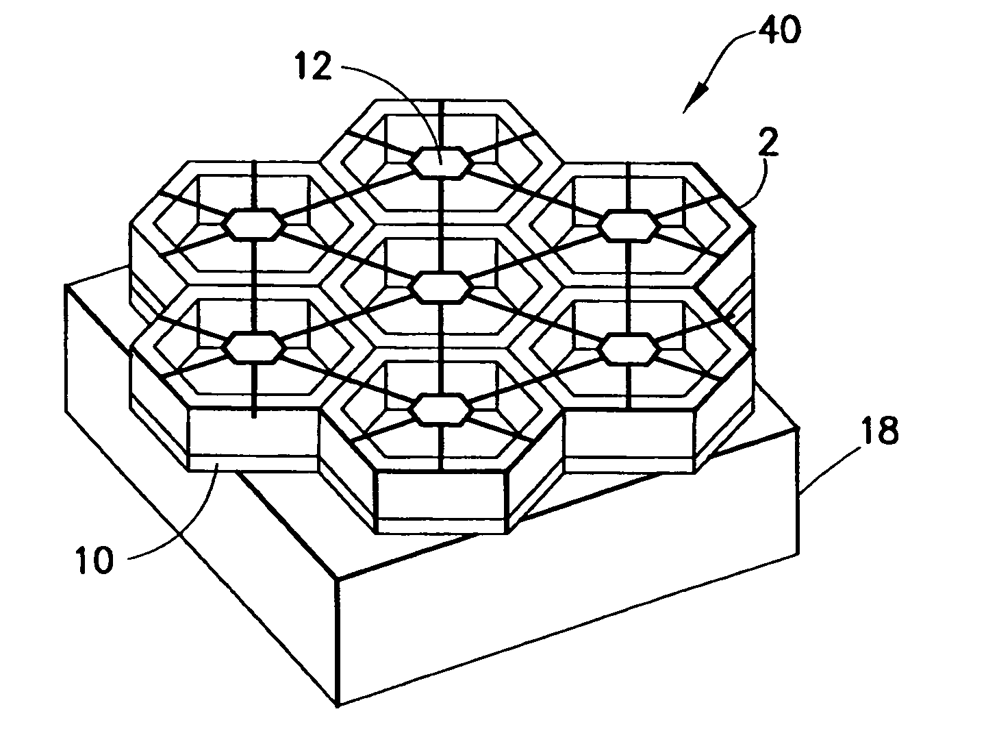
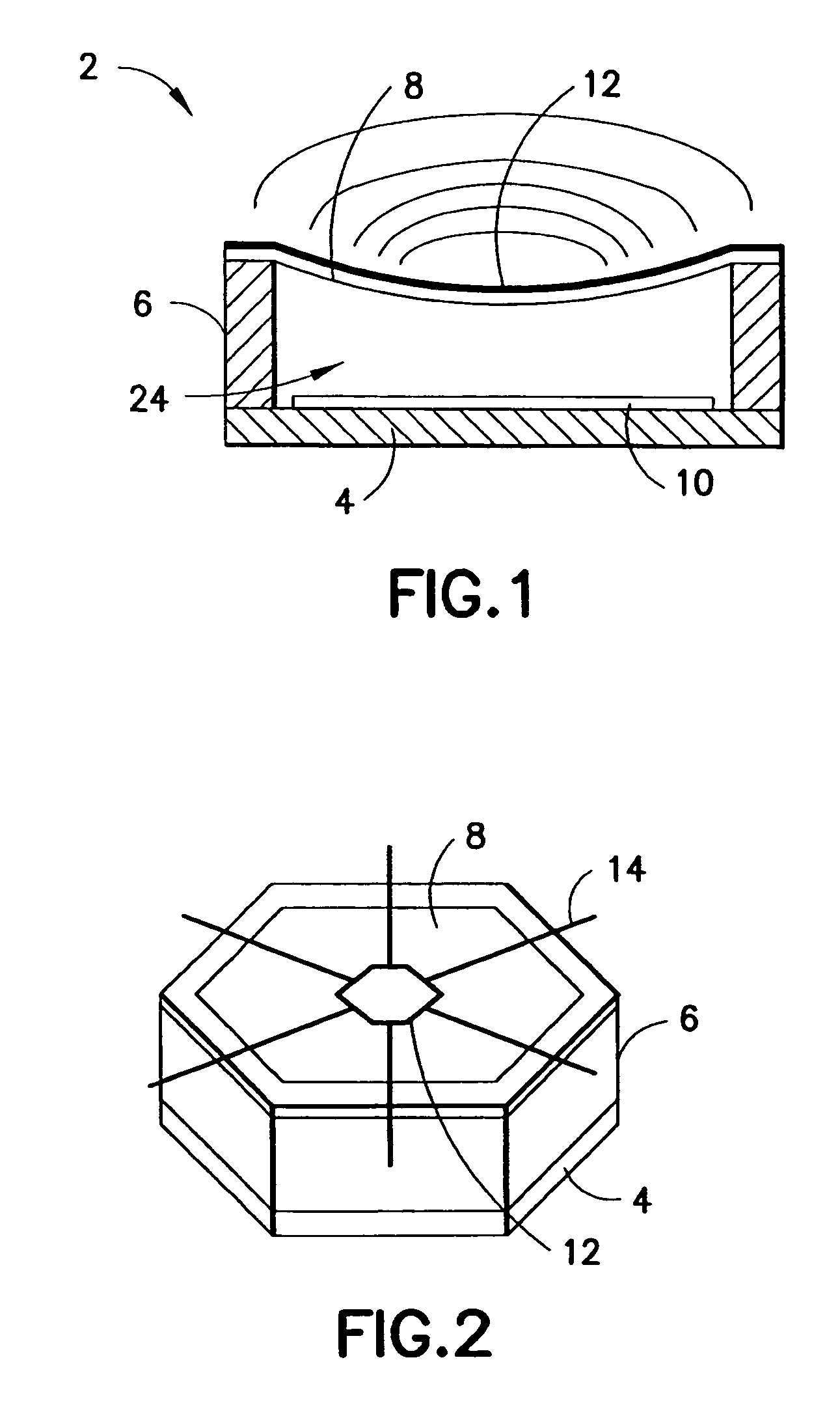
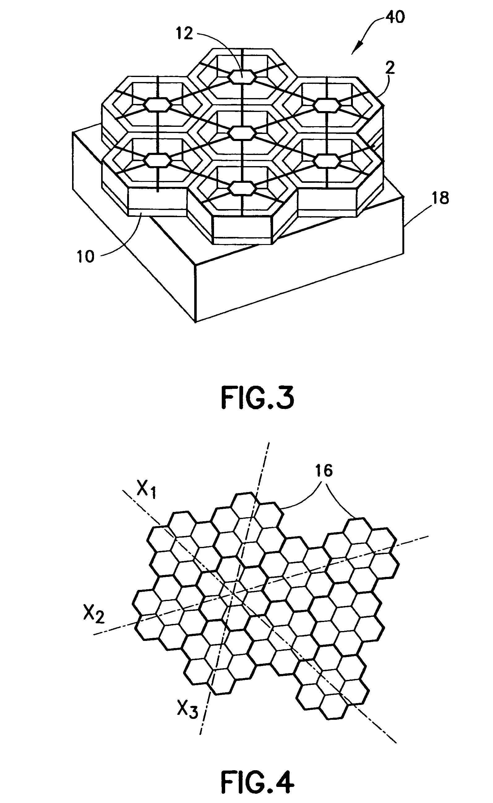
[0030]Referring to FIG. 1, a typical cMUT transducer cell 2 is shown in cross section. An array of such cMUT transducer cells is typically fabricated on a substrate 4, such as a heavily doped silicon (hence, semiconductive) wafer. For each cMUT transducer cell, a thin membrane or diaphragm 8, which may be made of silicon nitride, is suspended above the substrate 4. The membrane 8 is supported on its periphery by an insulating support 6, which may be made of silicon oxide or silicon nitride. The cavity 16 between the membrane 8 and the substrate 4 may be air- or gas-filled or wholly or partially evacuated. A film or layer of conductive material, such as aluminum alloy or other suitable conductive material, forms an electrode 12 on the membrane 8, and another film or layer made of conductive material forms an electrode 10 on the substrate 4. Alternatively, the bottom electrode can be formed by appropriate doping of the substrate.

[0031]Due to the micron-size dimensions of a typical cMU...


PUM

PropertyMeasurementUnit
symmetryaaaaaaaaaa
axes of symmetryaaaaaaaaaa
of symmetryaaaaaaaaaa

Abstract

An integrated circuit is fabricated by micromachining a hexagonal array of cMUT elements on top of a substrate comprising a hexagonal array of CMOS cells. Each cMUT element overlies a respective CMOS cell in one-to-one correspondence. During layout of the mask for micromachining the cMUT layer, either the hexagonal pattern or the alignment key is rotated until an axis of symmetry of the hexagonal pattern is aligned with an axis of the alignment key. Later, when the mask is superimposed on the CMOS substrate, the alignment key on the mask is aligned with an alignment key on the substrate. This ensures that the cMUT elements formed by optical lithography will be matched to the CMOS cells.

Description

STATEMENT REGARDING FEDERALLY SPONSORED RESEARCH & DEVELOPMENT[0001]The United States Government may have certain rights in this invention pursuant to U.S. Government Contract Number DAND17-02-1-0181 awarded by The U.S. Army Medical Research Acquisition Activity.BACKGROUND OF THE INVENTION[0002]This invention generally relates to the fabrication of micromachined ultrasonic transducers. In particular, the invention relates to the fabrication of ultrasonic transducer arrays on CMOS wafers.[0003]Recently semiconductor processes have been used to manufacture ultrasonic transducers of a type known as micromachined ultrasonic transducers (MUTs), which may be of the capacitive (cMUT) or piezoelectric (pMUT) variety. cMUTs are tiny diaphragm-like devices with electrodes that convert the sound vibration of a received ultrasound signal into a modulated capacitance. For transmission the capacitive charge is modulated to vibrate the diaphragm of the device and thereby transmit a sound wave.[000...

Claims


Application Information

Patent Timeline
Patent Type & Authority Patents(United States)
IPC IPC(8): A61B8/00G03F9/00B06B1/02B81B7/04B81C1/00H01L21/00H01L21/027
CPCB06B1/0292Y10T29/42
Inventor WODNICKI, ROBERT G.
Owner GENERAL ELECTRIC CO
Why Eureka
Try Eureka