
Low-jitter differential-to-single-ended data conversion circuits

a data conversion circuit and low-jitter technology, applied in logic circuits, multiple input and output pulse circuits, pulse techniques, etc., can solve the problems of leakage effects that tend to lower the voltage at the node, and achieve the effect of stabilizing the voltage on the node, lowering the voltage at the node, and stabilizing the current mirror and output signal

Inactive Publication Date: 2006-05-30
ALTERA CORP
View PDF15 Cites 19 Cited by
  • Summary
  • Abstract
  • Description
  • Claims
  • Application Information

AI Technical Summary

Benefits of technology

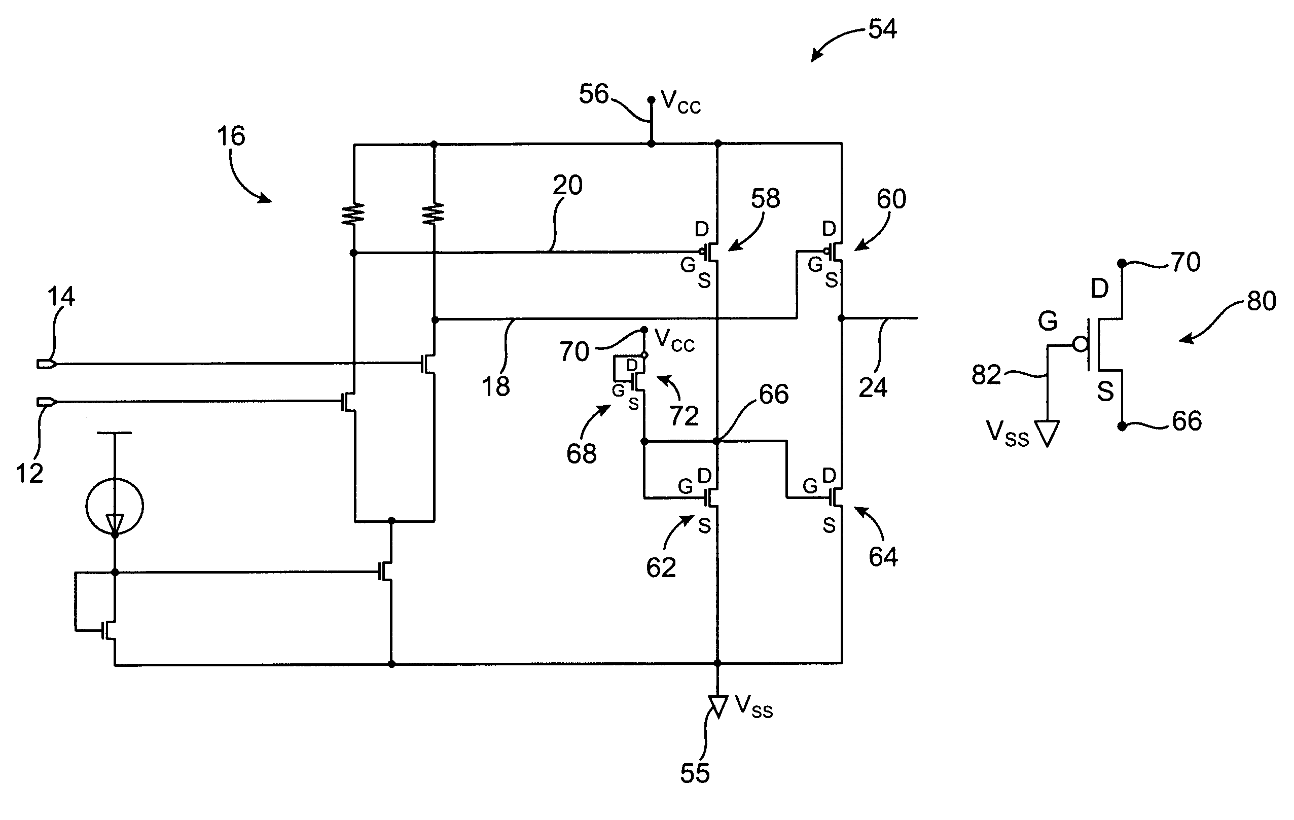
[0008]The NMOS transistors may be connected to form a current mirror circuit. The gates of the NMOS transistors are connected to a node to which the source of one of the PMOS transistors is also connected. When that PMOS transistor is off during the processing of differential data signals (e.g., digital ones), leakage effects tend to lower the voltage at the node. The differential-to-single-ended conversion circuit has a load that is connected to this node. The load supplies a current that offsets the leakage effects and that stabilizes the voltage on the node. This stabilizes the current mirror and output signal against fluctuations due to run-length variations in the differential input data. The differential-to-single-ended conversion circuit exhibits low-jitter and high temperature stability.

Problems solved by technology

When that PMOS transistor is off during the processing of differential data signals (e.g., digital ones), leakage effects tend to lower the voltage at the node.

Method used


Image

  • Low-jitter differential-to-single-ended data conversion circuits
  • Low-jitter differential-to-single-ended data conversion circuits
  • Low-jitter differential-to-single-ended data conversion circuits

Examples


Embodiment Construction

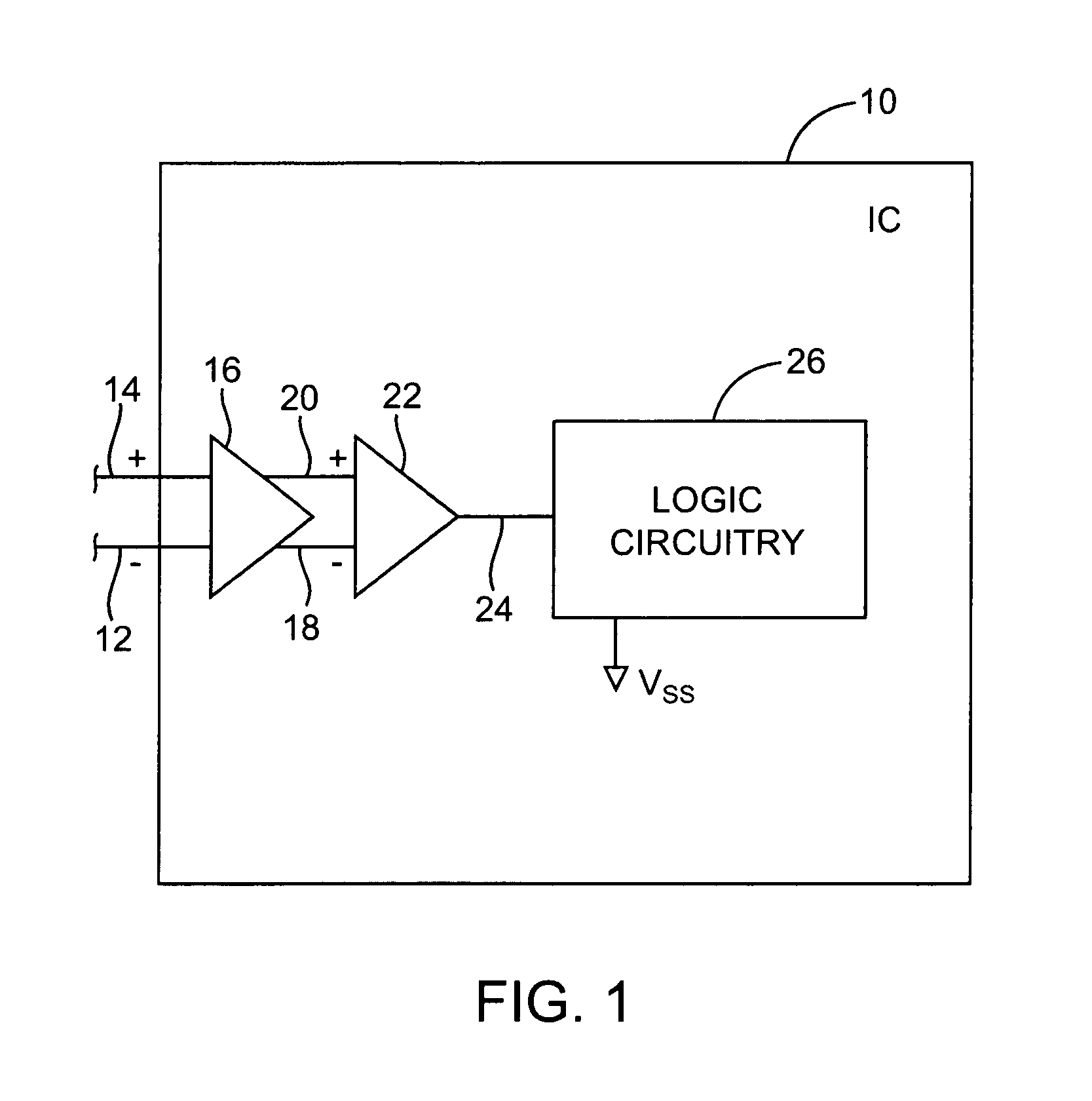
[0022]The present invention relates to circuitry for converting differential signals to single-ended signals for use on an integrated circuit. Differential signaling schemes use a pair of complementary signals that are referenced to each other. Differential signaling schemes are commonly used where high speed and good noise immunity are desired. For example, communications paths in a system backplane may use differential signaling.

[0023]Digital integrated circuits typically handle data internally in the form of single-ended signals. Single-ended signals are referenced to ground. If a single-ended signal has a high voltage (e.g., a voltage near a positive power supply voltage), that signal is said to be “high” (i.e., it represents a logic “1”). If a single-ended signal has a low voltage (e.g., a voltage near ground, that signal is said to be “low” (i.e., it represents a logic “0”).

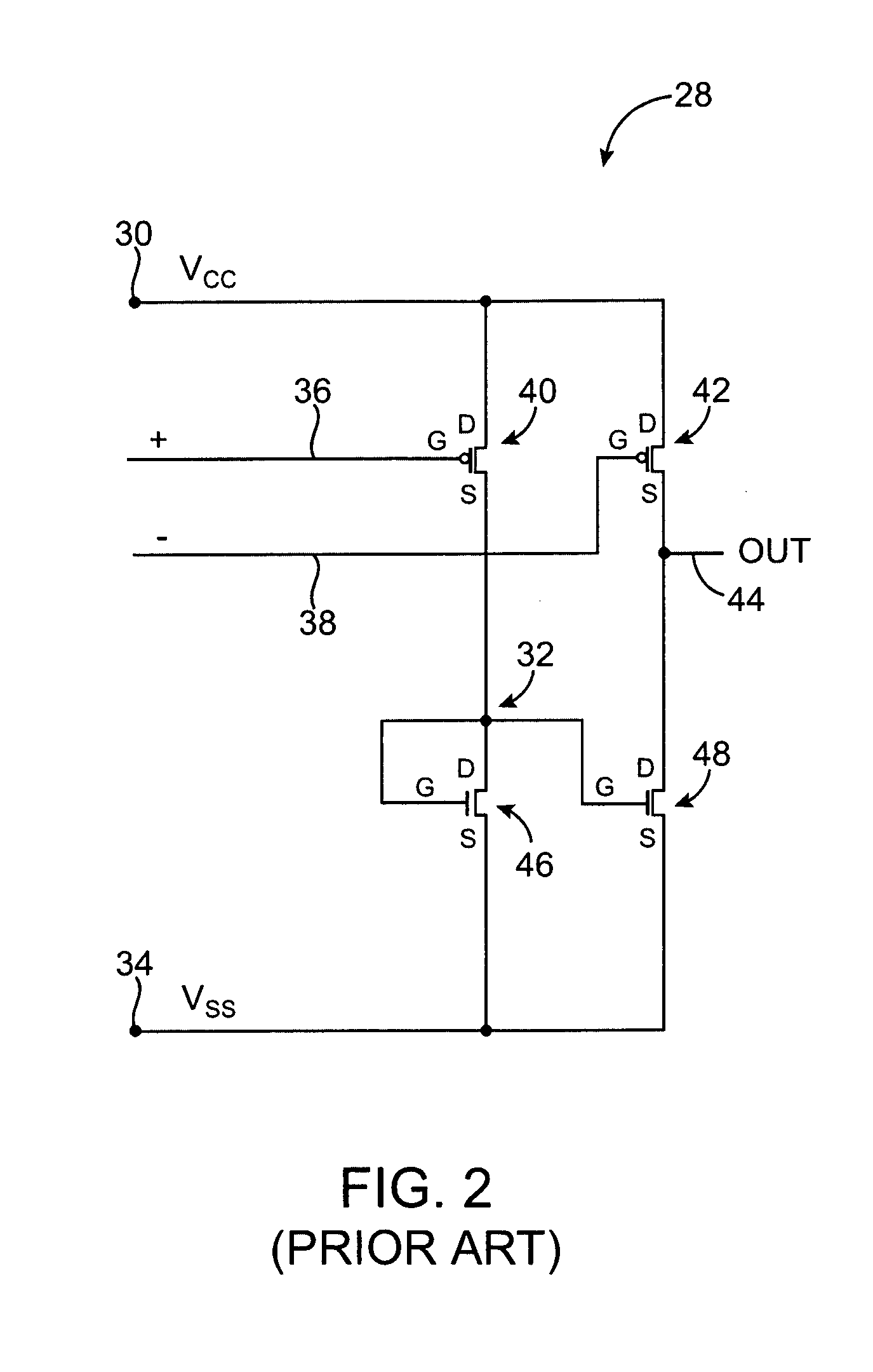
[0024]Differential-to-single-ended conversion circuitry (sometimes called level-shifting circuitry) is u...


PUM


Abstract

Circuitry is provided for converting differential digital data to single-ended digital data. Differential data signals have complementary pairs of signals that are referenced to each other. Single-ended signals are referenced to ground. The circuitry can be used on an integrated circuit to convert incoming differential data from a high-speed communications link to single-ended data for processing by internal logic on the integrated circuit. The operation of the circuitry can be stabilized using load circuitry that reduces temperature effects and jitter in the single-ended data.

Description

BACKGROUND OF THE INVENTION[0001]This invention relates to circuitry for converting differential data signals to single-ended data signals with low jitter.[0002]Differential signaling arrangements are used in a variety of environments such as in high-speed communications links. Differential signaling arrangements are generally more immune to noise than single-ended signaling schemes and can support higher data rates. In a differential arrangement, data is conveyed as complementary positive and negative signals. The positive and negative complementary signals are referenced to each other. In single-ended signaling arrangements, the same data may be represented by a single signal that is referenced to ground.[0003]Digital integrated circuits generally use single-ended logic schemes internally. When high-speed differential digital data is received from a high-speed differential communications link, it is necessary to use a conversion circuit to convert differential data to single-ended...

Claims


Application Information

Patent Timeline
IPC IPC(8): H03K5/22
CPCH03K19/018528
Inventor WONG, WILSON
Owner ALTERA CORP
Learn More