Reduced jitter charge pumps and circuits and systems utilizing the same

a charge pump and jitter reduction technology, applied in the field of phaselocked loops, can solve the problems of introducing dynamic jitter and skew into the system, unacceptable glitching currents or charges, and glitching also in voltage switching charge pumps, so as to reduce glitches, minimize current overshoot, and eliminate mismatch

Active Publication Date: 2006-05-30
CIRRUS LOGIC INC
View PDF13 Cites 16 Cited by
  • Summary
  • Abstract
  • Description
  • Claims
  • Application Information

AI Technical Summary

Benefits of technology

[0009]When utilized in phase-locked loop applications, charge pumps embodying the inventive principles minimize the injection of offset charge into the loop filter, and, consequently, frequency deviations in the phase-locked loop output signal. In particular, the voltages controlling the charge pump output differential pairs are optimized to minimize current overshoot. Further, this voltage swing is self-adjusting across a range of process corners. Finally, the present inventive principles provide, in some embodiments, for the elimination of mismatch between transistors of differing semiconductor types.

Problems solved by technology

However, the compensation scheme may, in itself, introduce voltage ripples and mismatch thereby introducing dynamic jitter and skew into the system.
This technique, however, requires that the MOSFETs be driven by rail to rail logic signals at their gates, which causes large step voltages to couple across the gate to drain capacitances and consequently unacceptable glitching currents or charges.
Glitching also occurs in voltage switching charge pumps due to inverter and gate delay mismatches and charge-sharing.
As a result, large MOSFETs are required in the differential pair, as well as large bias currents.

Method used


Image

  • Reduced jitter charge pumps and circuits and systems utilizing the same
  • Reduced jitter charge pumps and circuits and systems utilizing the same
  • Reduced jitter charge pumps and circuits and systems utilizing the same

Examples


Embodiment Construction

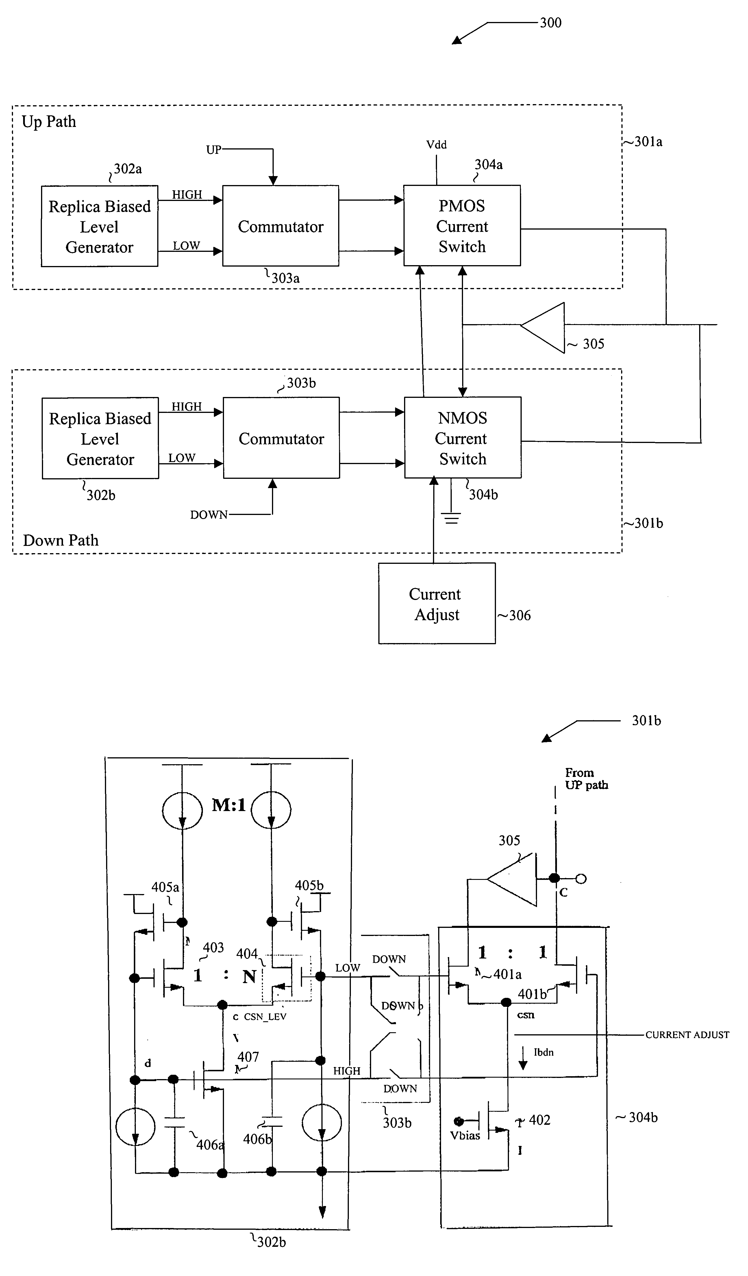
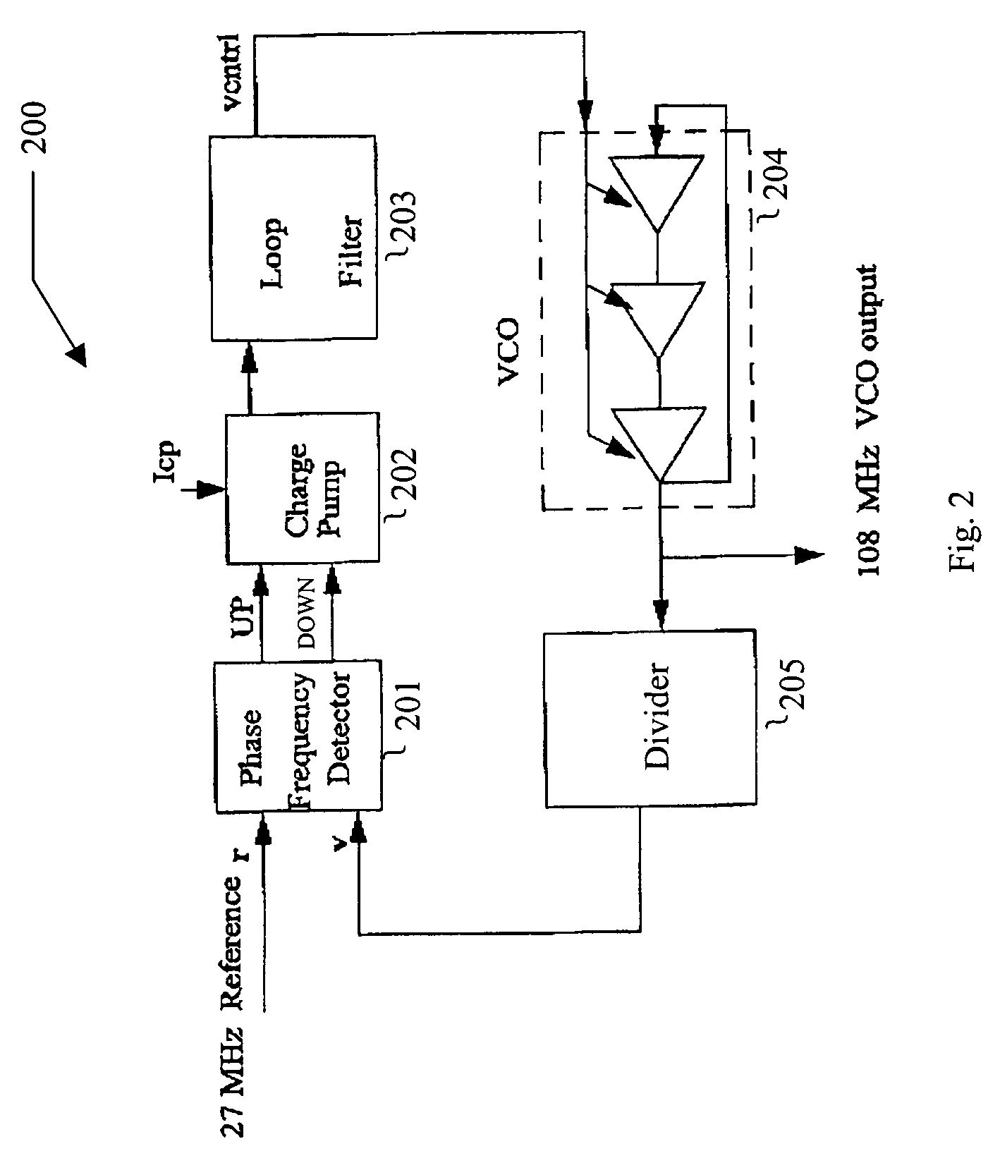
[0016]The principles of the present invention and their advantages are best understood by referring to the illustrated embodiment depicted in FIGS. 1–5 of the drawings, in which like numbers designate like parts.

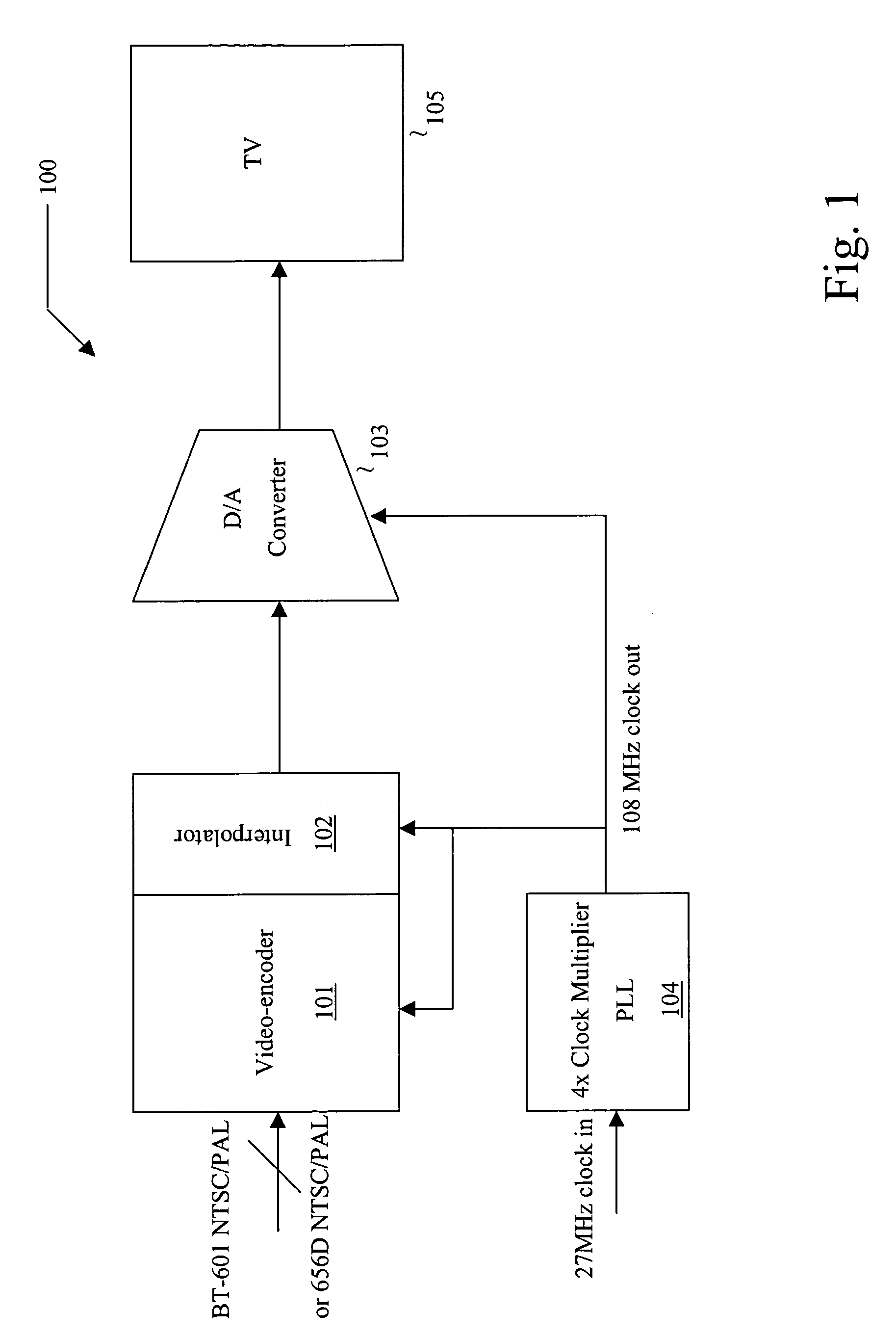
[0017]FIG. 1 is a high-level block diagram of a video-encoder system 100 representing one of numerous possible system level applications of the present inventive principles. Video-encoder system 100 includes a video-encoder 101 which receives digital television data, such as digital television data formatted in the International Telecommunications Union standards ITU-R-BT.601 or ITU-R-BT.656D for either the NTSC (National Television System Committee) or PAL (Phase Alternating Line) formats.

[0018]The incoming digital television data are converted by video-encoder 101, in conjunction with an interpolator 102 and a digital to analog converter (DAC) 103, into an analog output stream suitable for driving a television (TV) 105. Television 105 is, for example, a standard definition...


PUM


Abstract

A charge pump including a differential pair of transistors for controlling a current at a charge pump output node and a replica bias generator for selectively driving a first transistor of the differential pair of transistors into a fully-on state and a second transistor of the differential pair of transistors into a weak inversion state.

Description

FIELD OF INVENTION[0001]The present invention relates in general to phase-locked loops and in particular to reduced jitter charge pumps and circuits and systems utilizing the same.BACKGROUND OF INVENTION[0002]Phase-locked loops (PLLs) are widely used in electronic circuits to generate signals with closely controlled timing relationships. A few of the wide range of PLL applications include integral and fractional clock signal multiplication, clock signal recovery from a data bitstream, clock signal and data re-timing and de-skewing, and clock signal synthesis. Generally, the PLL is an indispensable building block in the design of any analog or mixed-signal circuits in which a precise timing relationship must be established between two signals.[0003]A number of different PLL designs are known in the art. In one particular design, a phase-frequency detector determines the deviation (error) from a desired timing relationship between the edges of a voltage controlled oscillator (VCO) gen...

Claims


Application Information

Patent Timeline
Patent Type & Authority Patents(United States)
IPC IPC(8): H03L7/06
CPCH03L7/0896H03L7/0995
Inventor SEN, SUBHAJITHODAPP, STEPHEN TIMOTHYMELANSON, JOHN LAURENCE
Owner CIRRUS LOGIC INC
Why Eureka
Try Eureka