MGT/FPGA clock management system

a clock management system and clock technology, applied in the field of communication systems, can solve the problems of high clock speed, limited bandwidth of prior art clock recovery circuits, and speed at which high-speed serial transceivers may operate without excessive jitter performance and/or noise performance, and achieve high data rate serial data, reduce or eliminate timing mismatches, and reduce the effect of high data ra

Active Publication Date: 2011-02-08
XILINX INC
View PDF114 Cites 10 Cited by
  • Summary
  • Abstract
  • Description
  • Claims
  • Application Information

AI Technical Summary

Benefits of technology

[0012]The present invention provides for a device and a method for processing high data rate serial data that reduces or eliminates mismatch between a reference clock and a high data rate serial data and the associated problems, including buffer overflow or underflow, that result therefrom. Generally, the invention includes circuitry for recovering a clock based on the high data rate input data stream and for providing the recovered clock to a circuit portion, for example, a portion of a field programmable gate array fabric, to enable the circuit portion to use either a reference clock or the recovered clock for subsequent processing. The invention specifically allows for different circuitry portions to utilize different clocks for a corresponding function that is being performed. Applications for the present invention are many but specifically include multi-gigabit transceiver, switching devices, protocol translation devices.
[0013]One embodiment of the present invention includes recovering a plurality of clocks from a corresponding plurality of serial data bit streams and using the plurality of recovered clocks to process each of the plurality of serial data bit streams in a corresponding functionality block. Another embodiment receives a high data rate serial data stream in a first protocol and translates the high serial data rate according to a recovered clock for the received high data rate serial data stream to a second protocol. Then, in one embodiment, the high data rate serial data stream in the second protocol is provided for transmission at the recovered clock rate. In an alternate embodiment, if the high data rate serial data stream is generated in the second protocol at a rate that is slightly different than the received data rate, the invention includes determining a corresponding clock and providing the high data rate serial data stream in the second protocol for transmission at a second recovered clock rate. It may be seen, therefore, that the invention includes circuitry and method for recovering and using a clock for a particular application to reduce timing mismatches. Further, the invention includes a device and method for recovering a plurality of clocks and performing a plurality of functions based on the plurality of recovered clocks concurrently.

Problems solved by technology

Higher clock speeds limit the usefulness of prior art clock recovery circuits that require precise alignment of signals to recover clock and / or data.
Some prior art designs are bandwidth limited.
The increased throughput demands are pushing some current integrated circuit manufacturing processes to their operating limits, where integrated circuit processing limits (e.g., device parasitics, trace sizes, propagation delays, device sizes) and integrated circuit (IC) fabrication limits (e.g., IC layout, frequency response of the packaging, frequency response of bonding wires) limit the speed at which the high-speed serial transceiver may operate without excessive jitter performance and / or noise performance.
For instance, switching from a CMOS process to a silicon germanium or gallium arsenide process would allow integrated circuit transceivers to operate at greater speeds, but at substantially increased manufacturing costs.
Currently, for most commercial-grade applications, including communication systems, such alternate integrated circuit fabrication processes are too cost prohibitive for widespread use.
Accordingly, designers of high data rate communication transceiver devices often have conflicting design goals that relate to the performance of the particular device.
Thus, a designer either cannot satisfy these mutually exclusive requirements (and therefore cannot support multiple protocols) or must design a high data rate transceiver device that can adapt according to the protocol being used for the communications.
One design challenge for serial data processing, especially for high data rate communications, relates to synchronization, and in particular to timing differences between a reference clock and high data rate serial stream.
Such differences can lead to buffer overflows / underflows, unnecessary delays and other complications.
The problem of synchronization mismatch become more acute in devices that conduct multi-gigabit serial data rates.
In these systems especially, but more generally in all serial communication systems, even a mismatch of one percent can lead to buffer overflows / underflows and other problems.
This problem of high data rate mismatch is a significant problem for any type of device or system that receives, processes or transmits high data rate serial data.

Method used


Image

  • MGT/FPGA clock management system
  • MGT/FPGA clock management system
  • MGT/FPGA clock management system

Examples


first embodiment

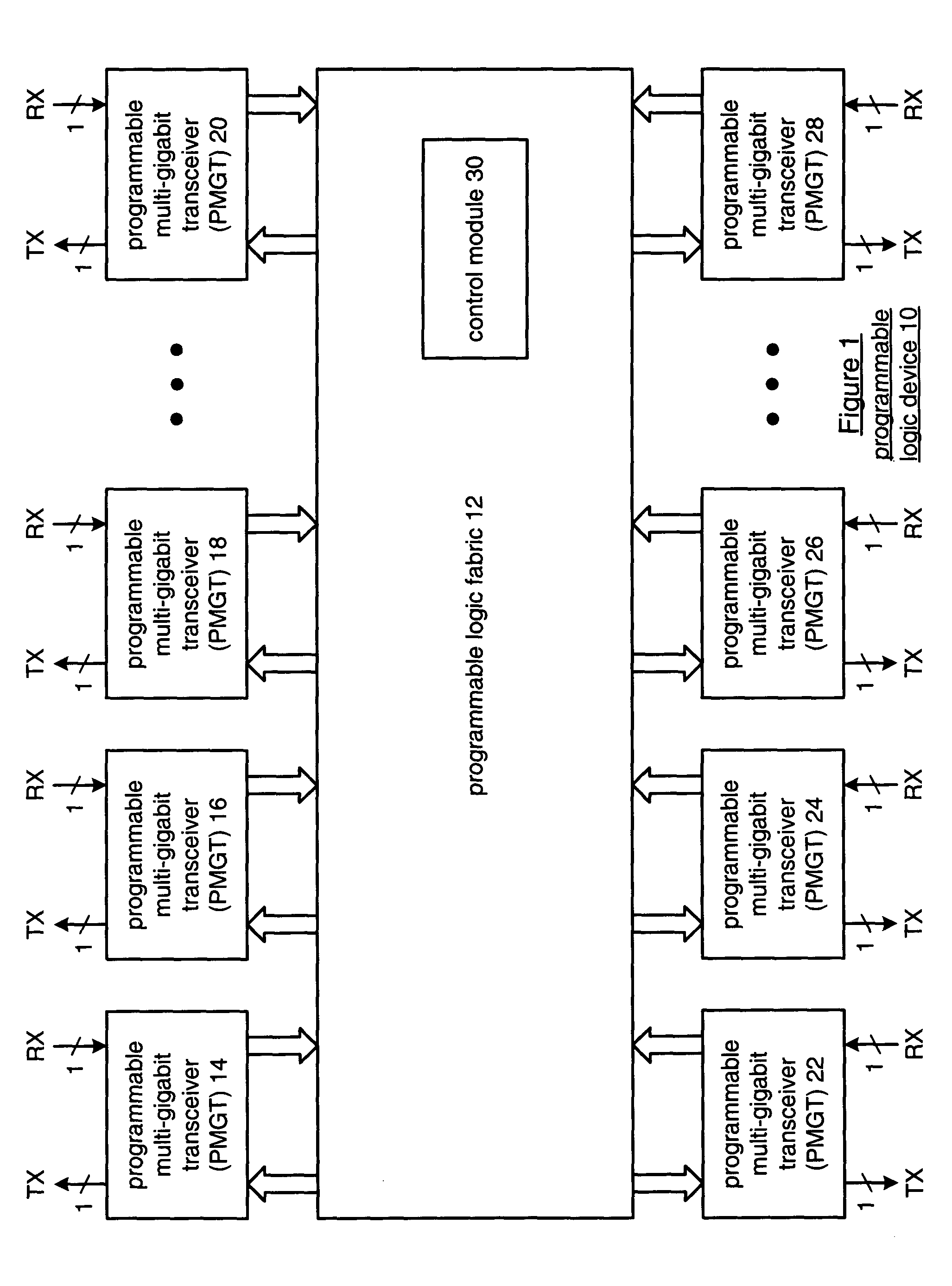
[0069]A plurality of methods of processing high data rate serial data utilizing the various embodiments of the transceivers illustrated in FIGS. 5-8 are illustrated in FIGS. 11-14. More specifically, FIG. 11 illustrates a method for processing high data rate serial data according to the invention. Initially, the method includes receiving a high data rate input data stream at the transceiver (step 250) and recovering a clock based on the high data rate input data stream (step 252). Thereafter, the transceiver method includes providing the recovered clock to an FPGA (or other programmable logic) fabric portion (step 254) and performing subsequent processing in the FPGA portion based on the recovered clock (step 256).

[0070]One embodiment of the inventive method further includes receiving the high data rate input data stream according to a first protocol and converting the high data rate input data stream to a second protocol based on the recovered clock (step 258). Once the data stream...

second embodiment

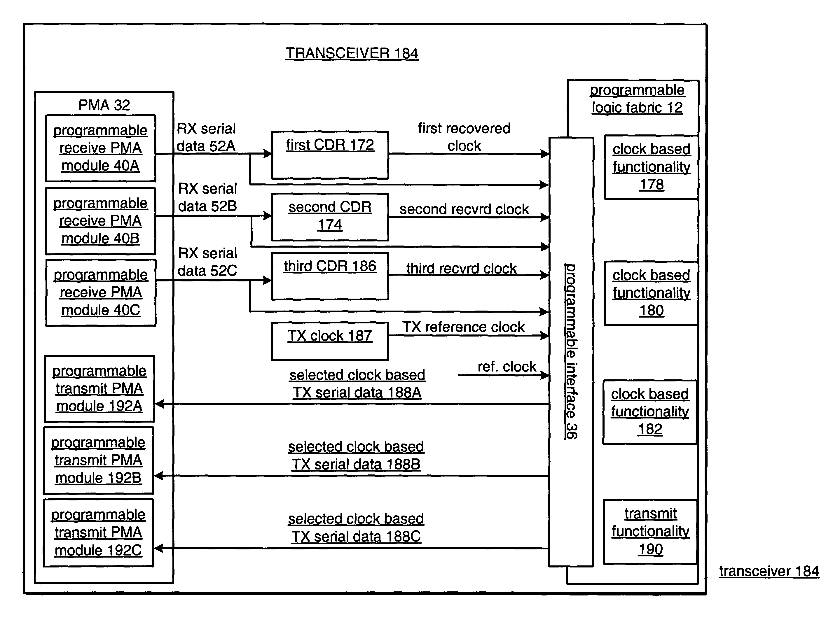
[0071]FIG. 12 illustrates a method of processing high data rate serial data according to the invention. The method initially includes receiving a first serial bit stream and recovering a clock from the first serial bit stream (step 262). Thereafter, the invention includes receiving a second serial bit stream and recovering a clock from the second serial bit stream (step 264). The transceiver of the present invention then provides the first and second recovered clocks and a reference clock to a circuit portion (step 266). Finally, the method includes, within the circuit portion, choosing among the first and second recovered clocks and the reference clock for subsequent processing for a specified functionality (step 268). As previously described, the circuit portion may be a fixed circuit or may be programmable logic fabric.

third embodiment

[0072]FIG. 13 illustrates a method of clock management according to the invention. The clock management in a processing block of a transceiver device includes receiving a first data stream and recovering a first clock based on the first data stream (step 270) and providing the first recovered clock to a first circuit portion (step 272). Additionally, the transceiver may receive a second data stream and recover a second clock based on the second data stream (step 274), and may provide the second recovered clock to a second circuit portion (step 276). The transceiver may also provide a reference clock to a third circuit portion (step 278). Finally, the processing block may concurrently perform processing functions in using one or more of the first and second recovered clocks and the reference clock (step 280).


PUM


Abstract

A device and a method for processing high data rate serial data includes circuitry for recovering a clock based on the high data rate input data stream and for providing the recovered clock to a circuit portion, for example, a portion of a field programmable gate array fabric, to enable the circuit portion to use either a reference clock or the recovered clock for subsequent processing. The invention specifically allows for different circuitry portions to utilize different clocks, including different recovered clocks, for corresponding functions that are being performed. Applications for the present invention are many but include multi-gigabit transceiver, switching devices, and protocol translation devices. More generally, the device and method provide for application specific clock references to be utilized in order to minimize or eliminate timing mismatch in serial data processing.

Description

BACKGROUND OF THE INVENTION[0001]1. Technical Field of the Invention[0002]This invention relates generally to communication systems and more particularly to clock recovery circuits used therein.[0003]2. Description of Related Art[0004]Communication systems are known to transport large amounts of data between a plurality of end user devices, which, for example, include telephones, facsimile machines, computers, television sets, cellular telephones, personal digital assistants, etc. As is known, such communication systems may be local area networks (LANs) and / or wide area networks (WANs) that are stand-alone communication systems or interconnected to other LANs and / or WANs as part of a public switched telephone network (PSTN), packet switched data network (PSDN), integrated service digital network (ISDN), or Internet. As is further known, communication systems include a plurality of system equipment to facilitate the transporting of data. Such system equipment includes, but is not lim...

Claims


Application Information

Patent Timeline
Patent Type & Authority Patents(United States)
IPC IPC(8): H04B1/38
CPCH04J3/0685H04L12/40013
Inventor GROEN, ERIC D.BOECKER, CHARLES W.BLACK, WILLIAM C.IRWIN, SCOTT A.KRYZAK, JOSEPH NEIL
Owner XILINX INC
Why Eureka
Try Eureka