Solid state imager with reduced number of transistors per pixel

a technology of transistors and imagers, applied in the field of solid-state imagers, can solve the problems of information destruction, high noise threshold, inherent high noise threshold, etc., and achieve the effects of reducing manufacturing scrap rate, increasing sensitivity in low-light level environments, and increasing manufacturing yield

Inactive Publication Date: 2006-06-06
DYNAMAX IMAGING
View PDF1 Cites 21 Cited by
  • Summary
  • Abstract
  • Description
  • Claims
  • Application Information

AI Technical Summary

Benefits of technology

[0015]It is another object to provide an imager that increases the amount of each pixel that is occupied by its photosensitive portion, without encountering other problems, such as fixed pattern noise.
[0016]It is another object to simplify the pixel structure of the solid state imager.
[0017]Likewise, it is an object to provide a solid-state imager that achieves a reduction in the number of FETs required, i.e., requiring on average a single FET per pixel.
[0020]The pixels of the group that share a common FETs can be in successive rows in the same column, or can be in adjacent columns in the same row. The group of pixels can comprise four pixels sharing a single output FET, or four pixels with two sharing one output FET and one reset FET and the other two sharing a second output FET and a second reset FET. By controlling the timing of the gate and reset signal, it is possible to “bin” or combine the photon-generated charge from the two pixels. Banning is useful for increasing sensitivity in low-light level environments. The imager can be configured as monochromatic or polychromatic (i.e., color), and the shared FET architecture of this invention can be used to great advantage where a Bayer pattern of color pixels is employed.
[0021]The solid-state imager of this advantage has the advantages of fewer FETs and fewer metallized strips or wires to carry signal and power to the pixels. This leaves more pixel area available for light collection, and also results in a significantly lower manufacturing scrap rate, i.e., higher manufacturing yield and reduced manufacturing costs.

Problems solved by technology

Pixels having only one transistor per pixel have been available only in passive imager designs, which have an inherent high noise threshold.
Passive pixel designs are pixels that do not buffer the photon-generated charge during read out, with the result that there is either high noise, such as with photodiodes and charge-injection devices (CIDs) or else the information is destroyed during read out, as in charge-coupled devices (CCDs).
However, because much of the available surface area of each pixel is occupied by these transistors, and by various power and control wires that have to cross the pixels, there is less area available for the active photosensor elements.
Active pixel sensors, or APS sensors suffer from fixed-pattern noise or FPN and typically require three or more transistors per pixel.
However, adding more transistors to each pixel reduces the fill factor and increases the unit cost for the imager.
Also pixel complexity has increased in many designs in order to provide additional pixel functions, such as shuttering capabilities for exposure control.
While micro-lenses permit smaller pixel size for a given set of process rules, the micro-lenses add cost to the wafer processing, and require yet another process step that can generate defects and reduce wafer yield.
Therefore, the micro-lens approach is less attractive than an alternative that would increase the area of each pixel that is available for collecting light.

Method used


Image

  • Solid state imager with reduced number of transistors per pixel
  • Solid state imager with reduced number of transistors per pixel
  • Solid state imager with reduced number of transistors per pixel

Examples


Embodiment Construction

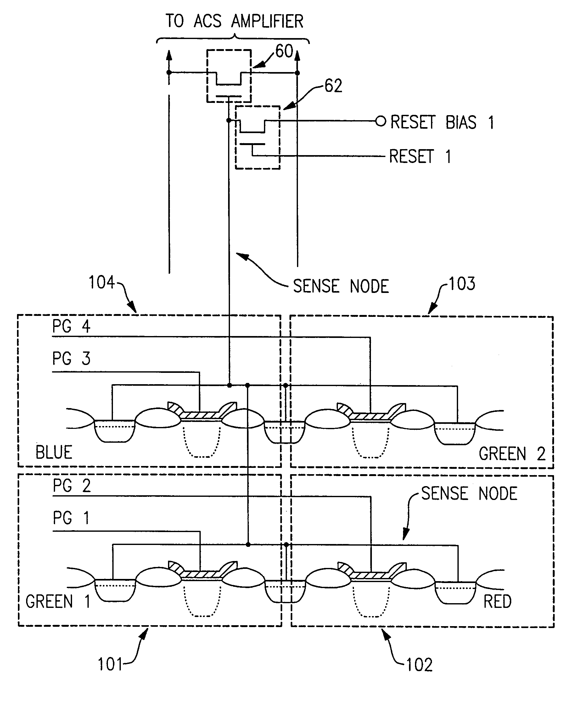
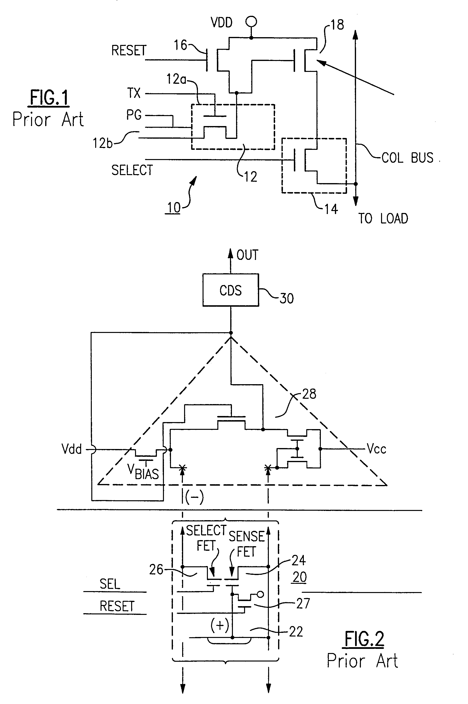
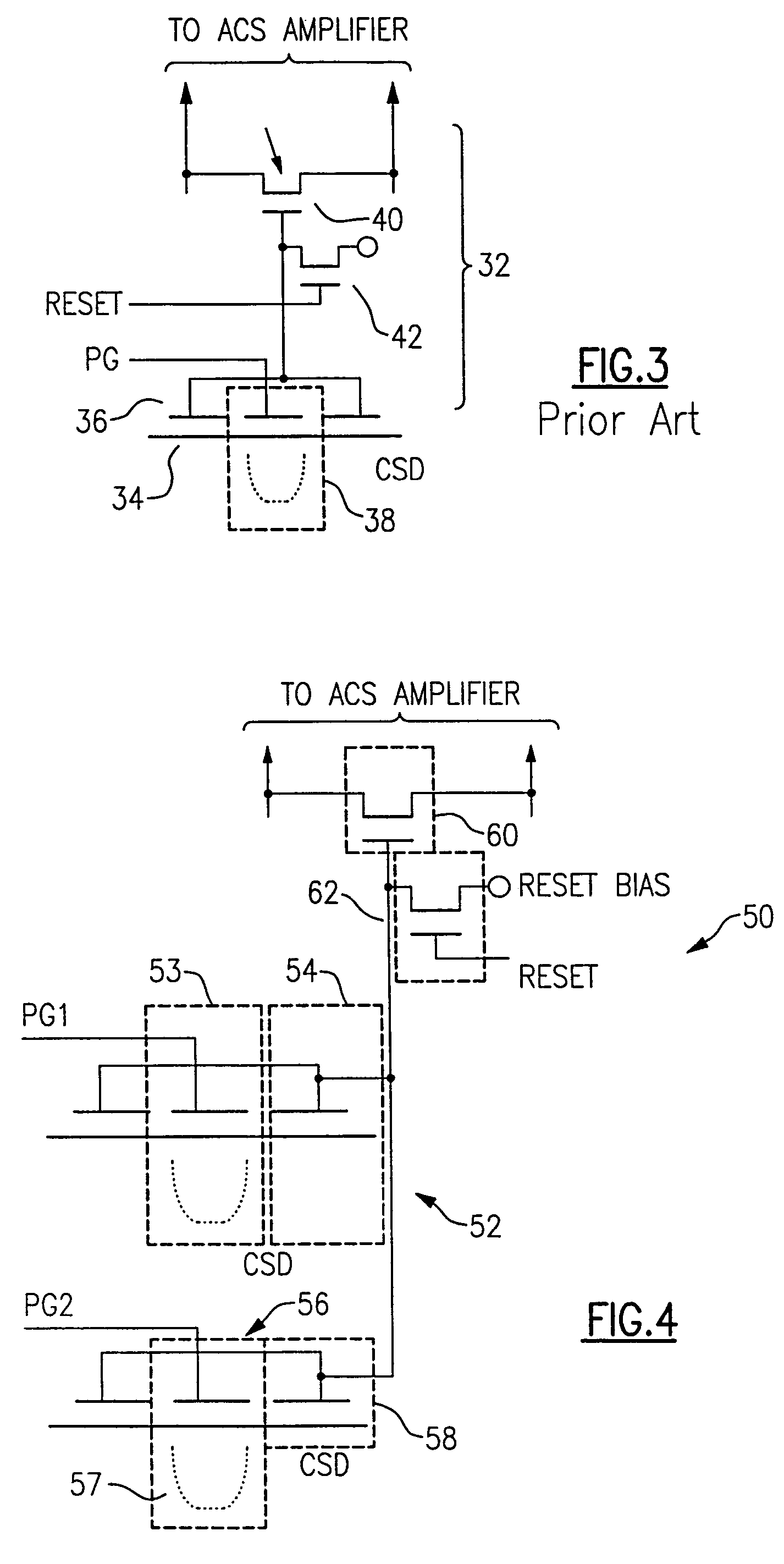
[0033]With reference now to the Drawing, and initially to FIG. 1 thereof, a CMOS imager 10, of the type that is known as an Active Pixel Sensor or APS, is shown here with a rather large number of components, including a photogate 12 which is the light sensitive member, with a transfer FET 12a, a row select transistor 14, a reset transistor 16, a sense FET 18, and various metallized leads including the row select lead SELECT, photogate lead PG, transfer lead TX, reset lead RESET, input drain voltage VDD, and output column bus COL BUS, which is connected to an output load. The APS imagers tend to have at least three and often many more FETs for each pixel, with pixel complexity increasing in many designs due to the addition of other pixel functions such as shuttering capabilities for exposure control. Even with only three FETs per pixel, a 1.3 megapixel imager will have 3.9 million transistors in the pixel array alone. The three transistors are a lower limit of complexity in the APS s...


PUM


Abstract

A solid state imager with pixels arranged in columns and rows has the pixels are configured into groups of at least a first pixel and a second pixel, each said group sharing a pixel output transistor having a sense electrode and an output electrode and a reset transistor having a gate coupled to receive a reset signal and an output coupled to the sense electrode of the associated shared pixel output transistor. Each of the pixels has a photosensitive element whose output electrode is coupled to the sense electrode of the shared pixel output transistor and a gate electrode coupled to receive respective first and second pixel gating signals. This configuration reduces the number of FETs to two transistors for each pair of pixels, and also can achieve true correlated double sampling correction of FPN.

Description

CONTINUING APPLICATION DATA[0001]This is a continuation in part of earlier patent application Ser. No. 09 / 768,124 filed Jan 23, 2001 now U.S. Pat. No. 6,633,029, which is a continuation in part of application Ser. No. 09 / 490,374, filed Jan. 24, 2000, now U.S. Pat. No. 6,590,198, Jul. 8, 2003, issued Jul. 8, 2003 which is a continuation in part of application Ser. No. 09 / 039,835, filed Mar. 16, 1998, now U.S. Pat. No. 6,084,229, Jul. 4, 2000 issued Jul. 4, 2000.BACKGROUND OF THE INVENTION[0002]This invention concerns solid state imagers, and in particular is directed to an improved configuration of the pixels within a given column of a solid state imager. The invention is more particularly concerned with a pixel configuration that reduces the number of FETs associated with each given pixel so as to maximize the area available for collection of light.[0003]Solid state image sensors are used in a wide variety of applications, and there has been much interest in pursuing low-cost, high-...

Claims


Application Information

Patent Timeline
Patent Type & Authority Patents(United States)
IPC IPC(8): H01J40/14H04N5/347H04N5/365H04N5/3745H04N9/07
CPCH01L27/14609H04N5/335H01L27/14641H04N5/363H04N5/37457H04N5/347H04N25/46H04N25/00H04N25/65H04N25/778
Inventor ZARNOWSKI, JEFFREY J.AMBALAVANAR, SAMUEL D.JOYNER, MICHAEL E.KARIA, KETAN V.
Owner DYNAMAX IMAGING
Why Eureka
Try Eureka