Scalable nano-transistor and memory using back-side trapping

a nano-transistor and memory technology, applied in the field of electromechanical circuits, can solve the problems of ineffective scaling of conventional front-floating gate memory structures, complex processing, and often quite dissimilar structure of logic and memory devices

Inactive Publication Date: 2006-06-06
CORNELL RES FOUNDATION INC
View PDF12 Cites 38 Cited by
  • Summary
  • Abstract
  • Description
  • Claims
  • Application Information

AI Technical Summary

Benefits of technology

[0006]According to an aspect of the invention, a new device structure is provided where charging and discharging occur in a trapping region formed by a stack of films that is placed on the back of a thin silicon channel. Uncoupling the charging mechanisms that lead to the memory function from the front gate transistor operation allows efficient scaling of the front gate. But significantly more important is a unique character of these devices: these structures can be operated both as a transistor and as a memory. The thin active silicon channel and the thin front oxide provide the capability of scaling the structure to tens of nanometers, and the dual function of the device is obtained by using two voltage ranges that are clearly distinct. At small voltages the structure operates as a normal transistor, and at higher voltages the structure operates as a memory device.

Problems solved by technology

The logic and memory devices and structures are usually quite dissimilar.
Such circuits, most of which are examples of systems-on-chip, require complex processing because of the different ways that logic and memory circuitry are implemented.
Conventional front-floating gate memory structures do not scale effectively due to gate-stack thickness limitations and due to inefficient coupling of hot carriers to front floating gates.
However, due to the structure of the conventional ONO-based memory device, the presence of a trapping layer between the channel of the device and the gate imposes restrictions on scaling of these devices because of the interdependence of electrostatics, voltages needed for adequate programming, speed, capture cross-sections, erasing speed and non-volatility.

Method used


Image

  • Scalable nano-transistor and memory using back-side trapping
  • Scalable nano-transistor and memory using back-side trapping
  • Scalable nano-transistor and memory using back-side trapping

Examples


Embodiment Construction

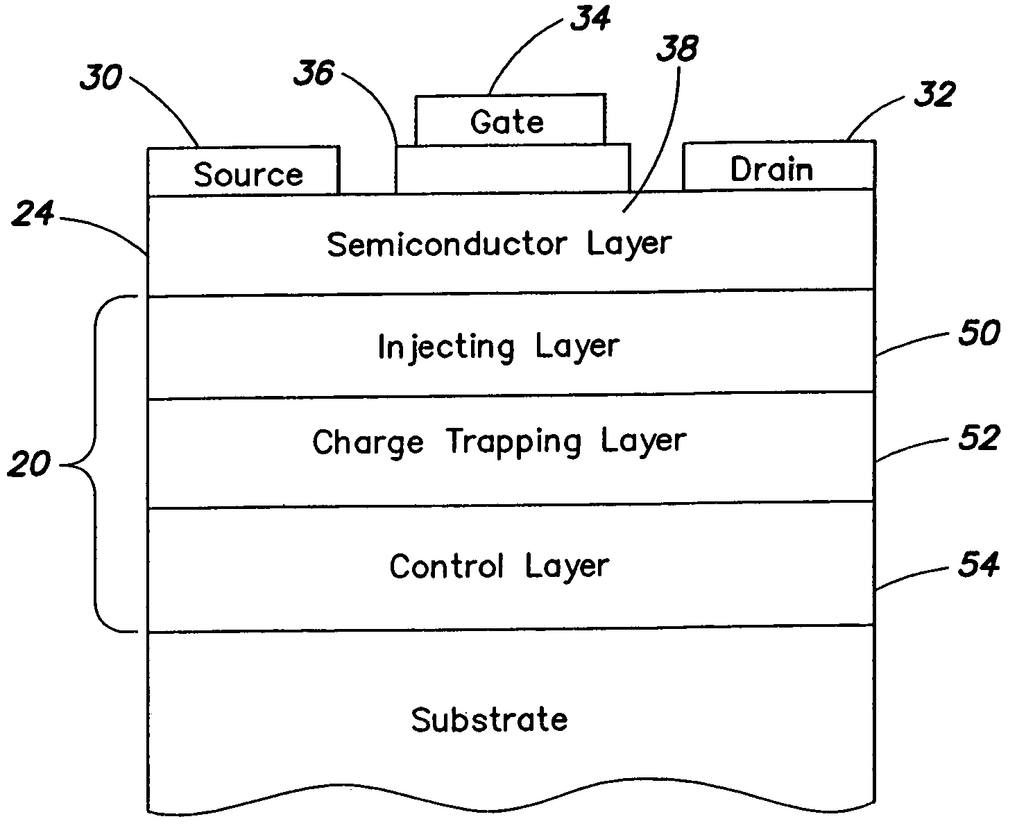
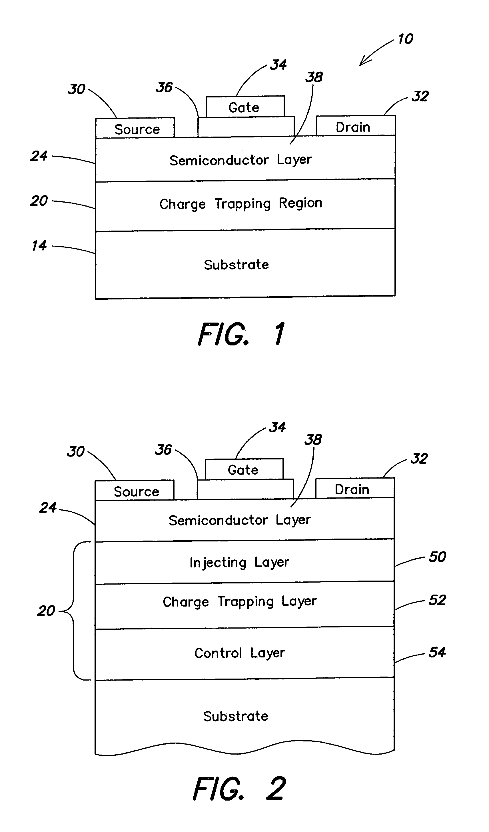
[0035]A schematic cross-sectional view of a semiconductor device 10 in accordance with an embodiment of the invention is shown in FIG. 1. A substrate 14 may be silicon or silicon having an oxide layer on an upper surface thereof, for example. However, substrate 14 is not limited to silicon. A charge trapping region 20 is formed on an upper surface of substrate 14. By way of example, charge trapping region 20 may be an insulating layer or a stack of insulating layers selected to perform a charge trapping function or a stack of insulating layers with nanocrystals embedded in it. The structure and operation of charge trapping region 20 are described in detail below. A semiconductor layer 24 is formed on an upper surface of charge trapping region 20. A source 30, a drain 32 and a gate 34 may be formed in semiconductor layer 34 to define a transistor. As is known in the art, gate 34 is spaced from semiconductor layer 24 by a gate oxide 36, and a channel 38 is defined in semiconductor lay...


PUM


Abstract

According to an aspect of the invention, a device structure is provided where charging and discharging occur in a trapping region formed by a stack of films that is placed on the back of a thin silicon channel. Uncoupling the charging mechanisms that lead to the memory function from the front gate transistor operation allows efficient scaling of the front gate. But significantly more important is a unique character of these devices: these structures can be operated both as a transistor and as a memory. The thin active silicon channel and the thin front oxide provide the capability of scaling the structure to tens of nanometers, and the dual function of the device is obtained by using two voltage ranges that are clearly distinct. At small voltages the structure operates as a normal transistor, and at higher voltages the structure operates as a memory device.

Description

CROSS REFERENCE TO RELATED APPLICATION[0001]This application claims priority based on provisional application Ser. No. 60 / 431,602, filed Dec. 6, 2002, which is hereby incorporated by reference.FIELD OF THE INVENTION[0002]This invention relates to electronic circuits and, more particularly, to semiconductor devices that can be operated both as a transistor and as a memory device. The invention also relates to methods of fabricating such devices, to semiconductor wafers in which such devices may be fabricated, to methods for fabricating such wafers, and to their use in integrated circuit applications.BACKGROUND OF THE INVENTION[0003]Many system-on-chip (SOC) applications and most microelectronic applications require the use of logic circuitry and memory circuitry simultaneously on the same integrated circuit chip. All stand-alone memory chips have both memory and logic together on them. The logic and memory devices and structures are usually quite dissimilar. One common example of mem...

Claims


Application Information

Patent Timeline
Patent Type & Authority Patents(United States)
IPC IPC(8): H01L27/01H01L21/28H01L21/336H01L21/762H01L27/10
CPCH01L21/28273H01L21/76254B82Y10/00H01L29/66825H01L27/10H01L29/40114
Inventor TIWARI, SANDIP
Owner CORNELL RES FOUNDATION INC
Why Eureka
Try Eureka