Micromirror for MEMS device

a micromirror and device technology, applied in the field of micromirrors, can solve the problems of low manufacturing yield, metal pits in the reflective layer, unstable contrast ratio of light reflected from the micromirror, etc., and achieve the effect of reducing the formation of voids or pits

Active Publication Date: 2006-06-06
TAIWAN SEMICON MFG CO LTD
View PDF12 Cites 9 Cited by
  • Summary
  • Abstract
  • Description
  • Claims
  • Application Information

AI Technical Summary

Benefits of technology

[0013]Accordingly, an object of the present invention is to provide a novel micromirror having enhanced reflective characteristics.
[0014]Another object of the present invention is to provide a novel micromirror characterized by reduced voids or pits.
[0013]Accordingly, an object of the present invention is to provide a novel micromirror having enhanced reflective characteristics.
[0018]Another object of the present invention is to provide a micromirror having a protective layer which functions as an effective mirror spacer etching stop layer.
[0013]Accordingly, an object of the present invention is to provide a novel micromirror having enhanced reflective characteristics.
[0018]Another object of the present invention is to provide a micromirror having a protective layer which functions as an effective mirror spacer etching stop layer.

Problems solved by technology

The DMD 10 shown in FIG. 1, while being an excellent engineering accomplishment, is very complex, costly to manufacture and has a low manufacturing yield.
One of the problems associated with the use of AlSiCu as the reflective layer 64 is that metal pits tend to form in the reflective layer 64.
Furthermore, the silicon tends to precipitate in the reflective layer 64, causing unstable contrast ratios of light reflected from the micromirror 32.
Moreover, the use of PEOX for the second protective layer 68 provides an unstable mirror spacer etching stop point, leading to compromised CID uniformity.

Method used


Image

  • Micromirror for MEMS device
  • Micromirror for MEMS device
  • Micromirror for MEMS device

Examples


Embodiment Construction

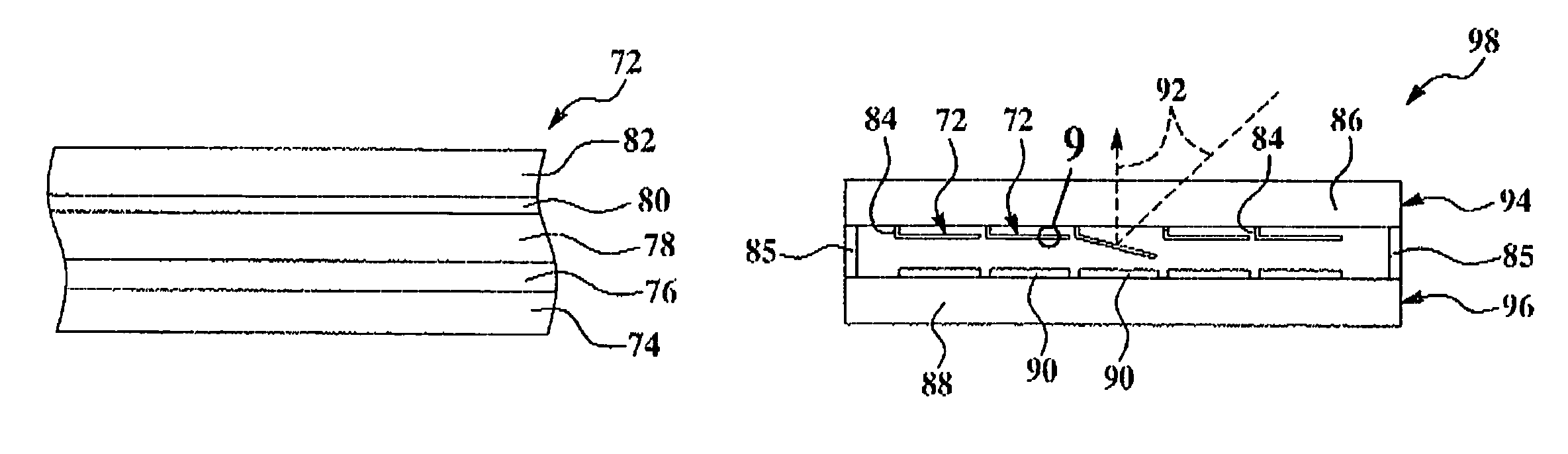
[0032]An illustrative embodiment of a micromirror 72 according to the present invention is shown in FIG. 9. The micromirror 72 includes a substrate 74, which is typically glass. The micromirror 72 may include a first protective layer 76 which may be any known protective layer including, but not limited to, silicon nitride, silicon oxide or silicon oxynitride. In one embodiment, the first protective layer 76 includes plasma enhanced silicon oxide (PEOX) or silicon oxide. The first protective layer 76 may have a thickness ranging from typically about 200 angstroms to typically about 600 angstroms. Preferably, the first protective layer 76 has a thickness of typically about 400 angstroms.

[0033]The micromirror 72 may include a reflective layer 78 overlying the first protective layer 76. As used herein, the description of a first layer “overlying” or “overlies” (or similar language) a second layer means that the first layer may be in direct contact with the second layer or that an additi...


PUM

PropertyMeasurementUnit
thickaaaaaaaaaa
thickaaaaaaaaaa
thickaaaaaaaaaa

Abstract

A micromirror which includes a substrate, a reflective layer comprising pure aluminum overlying the substrate and a protective layer comprising titanium nitride overlying the reflective layer is disclosed.

Description

FIELD OF THE INVENTION[0001]The present invention relates to micromirrors used in MEMS (micro-electro-mechanical systems). More particularly, the present invention relates to a novel multi-layered micromirror which includes a top titanium nitride (TiN) layer and a pure aluminum (Al) layer which underlies the TiN layer to reduce the incidence of defects in a micromirror.BACKGROUND OF THE INVENTION[0002]New advancements in projection systems utilize an optical semiconductor known as a digital micromirror device. A digital micromirror device chip may be the world's most sophisticated light switch. It contains an array of from about 750,000 to about 1.3 million pivotally-mounted microscopic mirrors. Each mirror may measure less than ⅕ of the width of a human hair and corresponds to one pixel in a projected image. The digital micromirror device chip can be combined with a digital video or graphic signal, a light source, and a projector lens so that the micromirrors reflect an all-digital...

Claims


Application Information

Patent Timeline
Patent Type & Authority Patents(United States)
IPC IPC(8): G02B26/00B05D5/06G02B26/08
CPCG02B26/0841
Inventor WANG, SHEN-PINGCHANG, YUH-HWACHEN, FEI-YUHHO, DAVIDCHEN, CHIA-CHIANG
Owner TAIWAN SEMICON MFG CO LTD
Why Eureka
Try Eureka