Transparent conductive film for transparent touch panel, transparent touch panel using transparent conductive film, and method of manufacturing transparent conductive film

a technology of transparent conductive film and touch panel, which is applied in the direction of oxide conductors, non-metal conductors, instruments, etc., can solve the problems of unstable input state of so-called light touch input that can be held for a slight load input, inability to obtain proper inputs, and more likely to occur that mis-inputs

Inactive Publication Date: 2006-06-13
NISSHA PRINTING COMPANY
View PDF15 Cites 21 Cited by
  • Summary
  • Abstract
  • Description
  • Claims
  • Application Information

AI Technical Summary

Benefits of technology

[0033]after coating or printing with the sol-gel material, performing an initially drying process; then performing an oxidation burning process at a temperature increasing rate o

Problems solved by technology

Accordingly, in a transparent touch panel using such transparent conductive films, because mutually contacting cross sections of transparent conductive films are formed generally triangular of grains, the so-called light touch input that an input state can be held for a slight-load input becomes unstable.
Further, in the case of successive inputs with an about 10 g load by using a pen or the like, there would occur frequently line breaks of continuous lines and mis-input portions as shown by A in FIG. 6 such that proper inputs cou

Method used


Image

  • Transparent conductive film for transparent touch panel, transparent touch panel using transparent conductive film, and method of manufacturing transparent conductive film
  • Transparent conductive film for transparent touch panel, transparent touch panel using transparent conductive film, and method of manufacturing transparent conductive film
  • Transparent conductive film for transparent touch panel, transparent touch panel using transparent conductive film, and method of manufacturing transparent conductive film

Examples


example 1

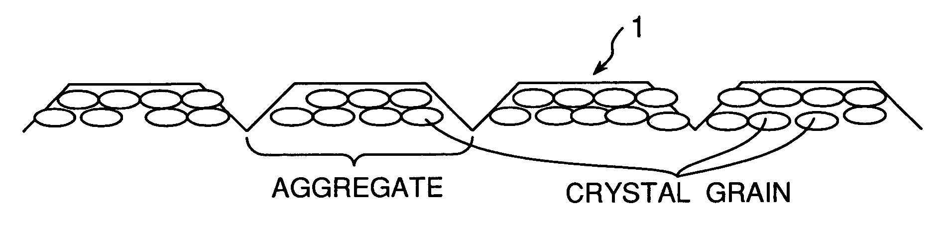
[0097]On a 20 μm thick polyethylene terephthalate film having an about 5 μm acrylic hard coat, an ITO film is formed as a transparent conductive film by sputtering process at a film formation temperature of 130° C. Further, an aging is performed at a temperature around 150° C., by which a transparent conductive film having a mean crystal grain size (R) distributed within a range of 40–60 nm is fabricated. A 125 μm polyethylene terephthalate film having an about 5 μm acrylic hard coat on its rear surface in advance is laminated on the hard coat surface of the transparent conductive film with an adhesive layer interposed therebetween.

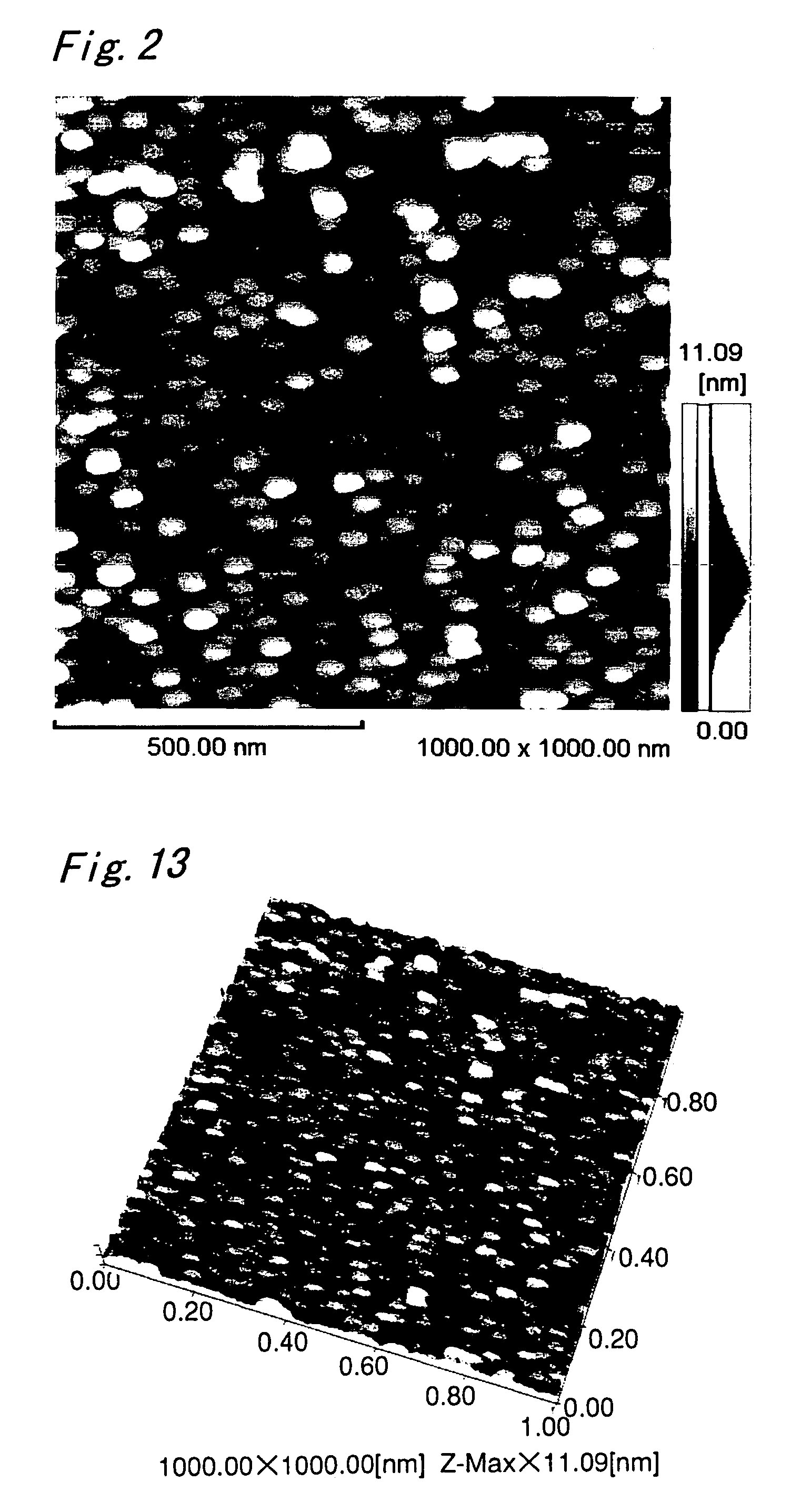
[0098]Also, by using, as the lower electrode substrate, a 1.1 mm thick glass dip-coated on both sides with SiO2, and with the substrate temperature set to 250° C., a 15 nm thick ITO film is formed as a transparent conductive film by sputtering process. As a result of observation by an atomic force microscope (SPM-9500 made by Shimadzu Seisakusho Kabushiki...

example 2

[0102]A transparent conductive film is formed on a polyethylene terephthalate film in the same way as in Example 1 except that the film formation temperature is set to 100° C. As a result of measuring the arithmetic mean roughness (Ra) of the surface of the transparent conductive film, the arithmetic mean roughness (Ra) is that 0.4 nm≦Ra≦1.2 nm, and the root-mean-square roughness (Rms) is 0.8 nm. In addition, the reference length is equal to a cutoff value used, and the evaluation length is a value obtained at 700 nm.

[0103]Also, a transparent conductive ink composition in which the ratio of indium to tin has been adjusted to {Sn / (Sn+In)}×100==20 wt % is printed on a SiO2-coated 300 mm×300 mm×1.1 mm soda glass substrate by the aforementioned thin film formation system (Angstromer™, In-Line type, made by Nissha Printing Co., Ltd.).

[0104]The glass substrate, after preliminarily dried by hot plate, is burned at 540° C. with a conveyor type atmosphere separating oven and subsequently coo...

example 3

[0109]A transparent conductive film is formed on a polyethylene terephthalate film in the same way as in Example 1 except that the film formation temperature is set to 150° C. and that an aging is performed at 150° C. for several hours. The mean crystal grain size (R) is distributed within a range of 40–100 nm. On the transparent conductive film surface, the arithmetic mean roughness (Ra) is that 1.1 nm≦Ra≦2.3 nm and the root-mean-square roughness (Rms) is 0.9 nm. In addition, the reference length is equal to a cutoff value used, and the evaluation length is a value obtained at 700 nm.

[0110]Also, a transparent conductive ink composition whose ratio of indium to tin has been adjusted to {Sn / (Sn+In)}×100=12 wt % is printed on a SiO2-coated 300 mm×300 mm×1.1 mm soda glass substrate by the aforementioned thin film formation apparatus (Angstromer™, In-Line type, made by Nissha Printing Co., Ltd.).

[0111]The glass substrate, after preliminarily dried by hot plate, is burned at 540° C. with...


PUM

PropertyMeasurementUnit
Temperatureaaaaaaaaaa
Nanoscale particle sizeaaaaaaaaaa

Abstract

In a transparent conductive film for use in a transparent touch panel in which a lower electrode and an upper electrode are stacked so as to be spaced from each other by spacers, the transparent conductive film being provided on an electrode substrate of at least one of the electrodes and thereby forming the electrode, the transparent conductive film has, in its surface shape, an arithmetic mean roughness (Ra) within a range of 0.4 nm≦Ra≦4.0 nm and a root-mean-square roughness (Rms) within a range of 0.6 nm≦Rms≦3.0 nm.

Description

TECHNICAL FIELD[0001]The present invention relates to a transparent conductive film for use in a transparent touch panel capable of performing stable, light touch inputs, to a transparent touch panel using the transparent conductive film, and to a method for fabricating a transparent conductive film. The transparent conductive film for use in a transparent touch panel, the transparent touch panel using the transparent conductive film, and the method for fabricating a transparent conductive film, according to the present invention are particularly suitable as a transparent conductive film for use in a transparent touch panel to be used as an input device by being laminated on a display screen of a flat display such as liquid crystal display devices, electroluminescent elements, plasma display devices, fluorescent character display tables, and field emission displays, and as a transparent touch panel using the transparent conductive film, and as a method for fabricating a transparent ...

Claims


Application Information

Patent Timeline
IPC IPC(8): B05D5/02B05D1/28B05D5/12C01G19/00G06F3/041G06F3/045
CPCC01G19/006G06F3/0414H01B1/08G06F3/045Y10T428/24355Y10T428/1055C09K2323/04G06F3/041
Inventor OMOTE, RYOUMEIINAKO, YOSHIHIDEMATSUKAWA, YOSUKESAKANE, MASAYASUNISHIKAWA, KAZUHIRO
Owner NISSHA PRINTING COMPANY
Why Eureka
Try Eureka