Process for fabricating a single-crystal substrate and integrated circuit comprising such a substrate

a technology of single crystal substrate and integrated circuit, which is applied in the direction of solid-state devices, basic electric elements, electric apparatus, etc., can solve the problems of destroying the crystal continuity of the surface oaf portion of the initial single crystal semiconductor substrate, the surface of the portion of the substrate, and the fabrication of semiconductor components, so as to ensure the planarity and surface homogeneity

Inactive Publication Date: 2006-06-13
STMICROELECTRONICS SRL
View PDF12 Cites 2 Cited by
  • Summary
  • Abstract
  • Description
  • Claims
  • Application Information

AI Technical Summary

Benefits of technology

[0008]The present invention provides a substrate with a single-crystal lattice which makes it possible to repair the local surface defects, to ensure planarity and surface homogeneity, and to ensure continuity of the single-crystal lattice of this surface.
[0015]The invention therefore makes it possible, for example, to form, on the surface, a single-crystal silicon layer which, being continuous with the rest of the initial silicon substrate offers a perfectly plane and uniform surface on which a single-crystal silicon layer free of crystal defects may be grown by epitaxy.
[0034]In general, according to the invention, the closing-off of the trenches with a “plug” of single-crystal material (for example silicon) allows, moreover, greater freedom with regard to the width and the nature of the trenches formed.
[0035]Furthermore this additional degree of freedom makes it possible, advantageously, to form electronic components buried in a substrate. Forming buried electronic components, such as capacitors or diodes, means that semiconductor devices formed subsequently on substrates with a uniform surface have a smaller footprint and exhibit greater performance and functionality.

Problems solved by technology

The processes for fabricating semiconductor components may destroy the crystal continuity of the surface oaf portion of the initial single-crystal semiconductor substrate.
Consequently, the surface of that portion of the substrate which is occupied by the trench, or more generally by any other local crystal defect, cannot be used to form semiconductor devices, particularly junctions or thin thermal oxides.

Method used


Image

  • Process for fabricating a single-crystal substrate and integrated circuit comprising such a substrate
  • Process for fabricating a single-crystal substrate and integrated circuit comprising such a substrate
  • Process for fabricating a single-crystal substrate and integrated circuit comprising such a substrate

Examples


first embodiment

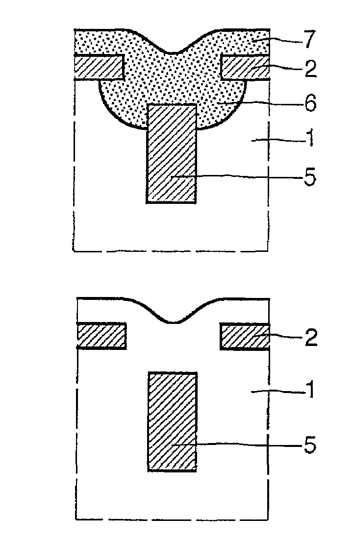
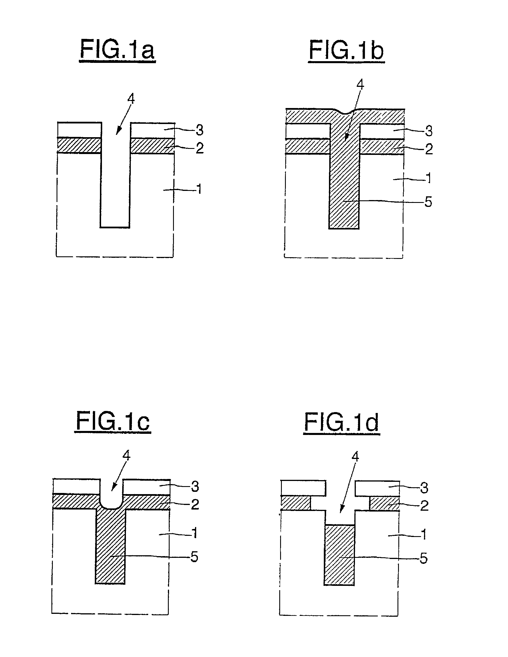
[0051] an isolating trench is formed for the purpose, for example, of separating contiguous buried layers of opposite conductivity.

[0052]Thus, according to this embodiment of the process of the invention, the trench 4 is filled with a dielectric material. As dielectric material, it is preferred to choose silicon oxide.

[0053]The filling of the trench with silicon oxide 5 maybe carried out in various conventional ways.

[0054]It is conceivable to deposit silicon oxide as a conformal coating, as illustrated in FIG. 1b. The oxide is therefore also deposited over the entire surface of the wafer.

[0055]It is preferable, however, to use the deposition of silicon oxide by thermal oxidation, as illustrated in FIG. 1c. Firstly, this involves a method more suited to the presence of possibly narrow trenches. Secondly, a denser oxide is obtained than with the conformal coating.

[0056]Moreover, if the silicon oxide grows only on the silicon, only the trench 4, slightly widened by oxidation of the sil...

second embodiment

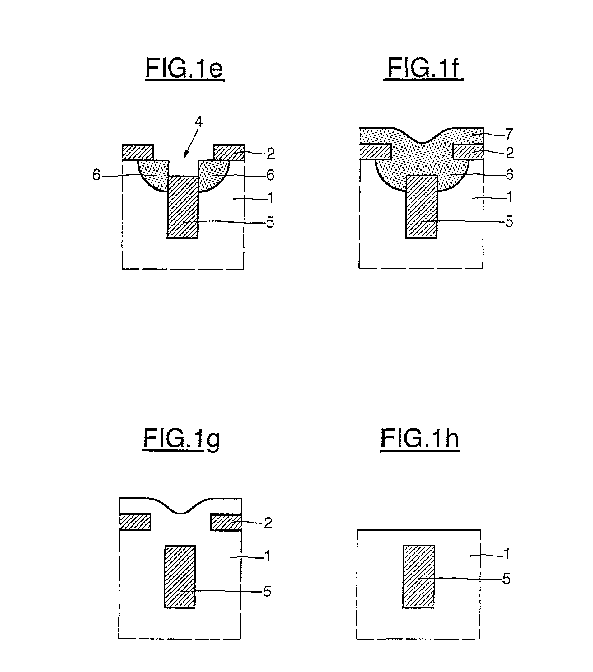
[0066] it is possible to produce a silicon substrate which has its surface made uniform according to the process of the invention and which includes a buried capacitor formed in a trench.

[0067]To produce such a substrate, a trench 4 is firstly formed as previously in the substrate 1, as illustrated in FIG. 1a. Next, a controlled thermal oxidation is carried out so as to form a silicon oxide layer 8 having a thickness of between 40 and 1000 Å, preferably between 50 and 300 Å, on the walls of the trench 4, obtaining the device illustrated in FIG. 2a.

[0068]Next, highly doped polycrystalline silicon 9 is deposited on the wafer so as to fill the trench 4. The doping of the silicon is carried out in situ.

[0069]A device like that illustrated in FIG. 2b is obtained.

[0070]Next, according to the process of the invention, the previously deposited polycrystalline silicon 9 is etched, so as at least to remove it from the surface of the wafer. Moreover, this etching is carried out until the poly...

third embodiment

[0080] it is also possible to form a buried diode in a silicon substrate, the surface of which is planarized as in the process of the invention, for the purpose of homogeneous epitaxy allowing electronic components to be produced.

[0081]According to this embodinent, highly doped polycrystalline silicon 10 is deposited in a trench formed as previously.

[0082]According to the embodiment illustrated in FIG. 3a, an n-doped substrate 1 and p+-doped polycrystalline silicon 10 have been envisioned. It is important to note however, that opposite conductivities also fall within the true scope and spirit of the invention.

[0083]Next, the polycrystalline silicon layer 10 formed on the surface is removed using standard methods. The removal of the polycrystalline silicon 10 is continued until a fill level below the surface of the substrate 1 is obtained.

[0084]This step is followed, according to the process of the invention, by a controlled deoxidation. This deoxidation is more fully described above...


PUM

PropertyMeasurementUnit
thicknessaaaaaaaaaa
thicknessaaaaaaaaaa
depthaaaaaaaaaa

Abstract

An initial single-crystal substrate 1 having, locally and on the surface, at least one discontinuity in the single-crystal lattice is formed. The initial substrate is recessed at the discontinuity. The single-crystal lattice is amorphized around the periphery of the recess. A layer of amorphous material having the same chemical composition as that of the initial substrate is deposited on the structure obtained. The structure obtained is thermally annealed in order to recrystallize the amorphous material so as to be continuous with the single-crystal lattice of the initial substrate.

Description

CROSS REFERENCE TO RELATED APPLICATIONS[0001]This application is based upon and claims priority from prior French Patent Application No. 0100414, filed Jan. 12, 2001, the disclosure of which is hereby incorporated by reference in its entirety.BACKGROUND OF THE INVENTION[0002]1. Field of the Invention[0003]The present invention generally relates to the field of integrated circuits, and more particularly to the production of an initial single-crystal substrate, for example made of silicon, having a discontinuity in the single-crystal lattice, such as a buried trench, for the epitaxial growth of a homogeneous single-crystal silicon layer.[0004]2. Description of Related Art[0005]The processes for fabricating semiconductor components may destroy the crystal continuity of the surface oaf portion of the initial single-crystal semiconductor substrate. This is especially the case during the formation of trenches. The trenches are subsequently filled so as to produce a dielectric insulation, ...

Claims


Application Information

Patent Timeline
Patent Type & Authority Patents(United States)
IPC IPC(8): H01L21/20H01L21/76H01L21/205H01L21/329H01L21/762H01L21/822H01L27/04H01L29/861
CPCH01L21/76235H01L21/2022H01L21/02667H01L21/0262H01L21/02381H01L21/02488H01L21/02598H01L21/02502H01L21/02532
Inventor MENUT, OLIVIERGRIS, YVON
Owner STMICROELECTRONICS SRL
Why Eureka
Try Eureka