Semiconductor device having balanced circuit for use in high frequency band

a balanced circuit and semiconductor technology, applied in the field of semiconductor devices, can solve the problems of high cost, disadvantageous size of devices having such amplifiers, and relatively heavy weight, and achieve the effects of reducing the size, weight and cost of semiconductor devices, and reducing the variation of rf characteristics depending on the accuracy of component alignmen

Active Publication Date: 2006-06-13
MURATA MFG CO LTD
View PDF7 Cites 25 Cited by
  • Summary
  • Abstract
  • Description
  • Claims
  • Application Information

AI Technical Summary

Benefits of technology

[0013]In the above configuration, both balanced circuits of each matching circuit are connected at a virtual grounding point, which can be used as a grounding point sensitive to the RF characteristics. Therefore, variations in ground inductance or the influence of ...

Problems solved by technology

The device having such an amplifier is disadvantageously large in size, relatively heavy, and high in cost.
Moreover, in the conventional device, the chip components and the like are mounted by solder on the wirings, and therefore an error of alignment or variations in high-frequency characteristics (RE characteristics) can disadvantageously be increased.
In ...

Method used


Image

  • Semiconductor device having balanced circuit for use in high frequency band
  • Semiconductor device having balanced circuit for use in high frequency band
  • Semiconductor device having balanced circuit for use in high frequency band

Examples


first embodiment

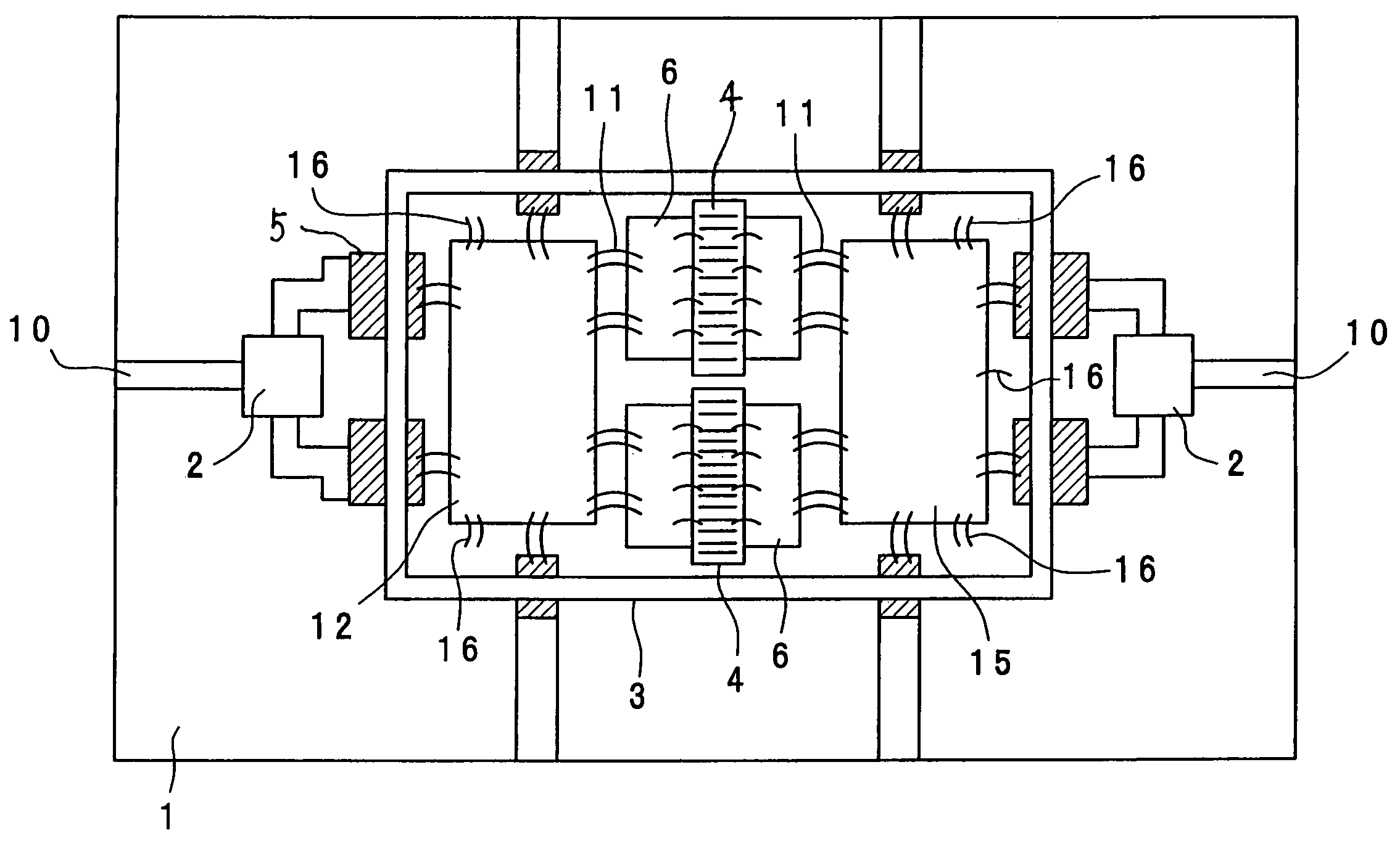
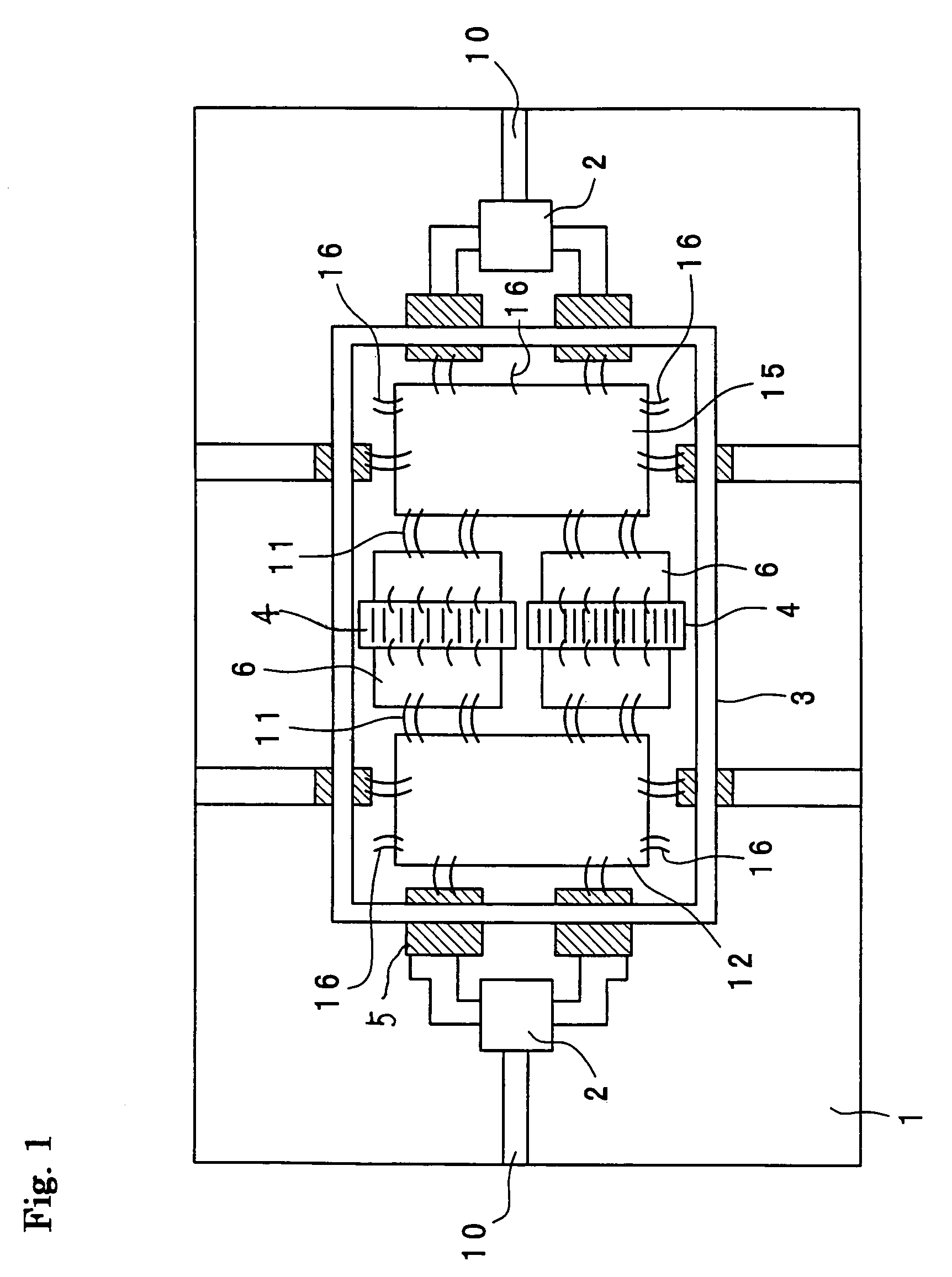
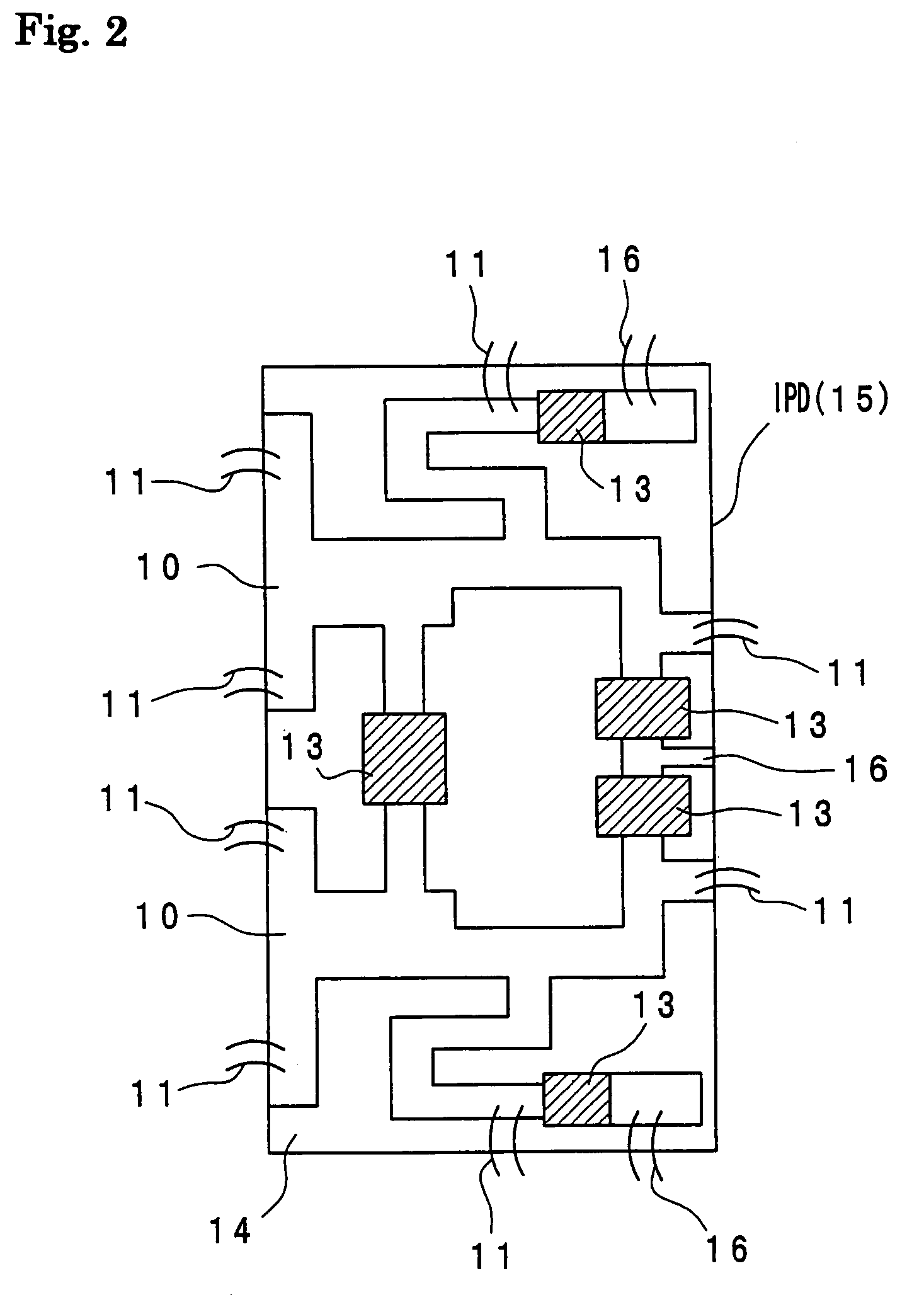
[0031]Referring to FIGS. 1 to 3, a first embodiment of the present invention is described below. FIG. 1 is a top view of the semiconductor device according to the first embodiment of the present invention; FIG. 2 is a top view of an output-side balanced matching circuit thereof, and FIG. 3 is an equivalent circuit diagram thereof.

[0032]The illustrated structure shows a push-pull high-power amplifier which is generally used in a high frequency band of 0.8 to 2.4 GHz. In FIG. 1, reference numeral 1 represents a housing of a PCB board (i.e., an insulating board) on which circuit components are mounted. Reference numeral 2 represents a balun, which is a passive distributed constant circuit used for connection (conversion) from a balanced line to an unbalanced line and vice versa. Reference numeral 3 represents a package. Reference numeral 4 represents a high-frequency amplifying semiconductor chip which is comprised of a field effect transistor (hereinafter, referred to as “FET”).

[0033]...

second embodiment

[0049]Referring to FIGS. 7 and 8, a second embodiment of the present invention is described below. FIG. 7 is a top view of an output-side IPD of the semiconductor device according to the second embodiment of the present invention; and FIG. 8 is a diagram showing an equivalent circuit thereof. In the first embodiment, the matching circuit comprises serial L1, L2 and L3 and ground capacitors C1 and C2. In contrast thereto, in the second embodiment, the matching circuit includes a capacitor C4 and a ground inductor L5 in serial, and the inductor L5 connects both channel matching circuits.

[0050]In the configuration as shown in FIGS. 7 and 8, the balanced circuits include the upper circuit and the lower circuit, which are different in phase by 180 degrees from each other. Therefore, the midpoint of the inductor L5 connecting both matching circuits provides a virtual grounding point, and the device can operate as if it is grounded at a half of the inductance L5. Such grounding can be idea...

third embodiment

[0053]Referring to FIGS. 9 to 11, a third embodiment of the present invention is described below. FIG. 9 is a top view of the semiconductor device according to the third embodiment of the present invention; FIG. 10 is a top view of an output-side balun-containing IPD thereof, and FIG. 11 is a diagram showing an equivalent circuit of the IPD as shown in FIG. 10.

[0054]In FIGS. 9 to 11, reference numeral 20 represents an input-side balun-containing IPD, and 21 an output-side balun-containing IPD. In the third embodiment, the balun 2 is included in each of the IPDs 20 and 21 on the input and output sides.

[0055]Since the balun 2 is formed on the substrate in the IPD, the device can further be reduced in size, weight and cost as compared with the first embodiment. In this configuration, the balun or the matching circuit does not have to be directly formed on the PCB board 1. The elements such as the balun and the matching circuit may be mounted on a package 3 and formed into a semiconduct...


PUM


Abstract

A semiconductor chip for amplification is connected between input-side and output-side matching circuits, and each of matching circuits includes balanced circuits which receive signals different in phase by 180 degrees, divided from an input signal. The balanced circuits are connected at a virtual grounding point, which is used as a grounding point sensitive to RF characteristics in an IPD. Thus, a semiconductor device can be free from influence of variations of grounding wires and can be reduced in size, weight, and cost.

Description

BACKGROUND OF THE INVENTION[0001]1. Field of the Invention[0002]The present invention generally relates to a semiconductor device, and particularly to a semiconductor device having a balanced circuit for use in a high frequency band of 800 MHz or higher.[0003]2. Description of the Related Art[0004]In a conventional semiconductor device having a plurality of IC chips mounted on one package, an intermediate electrode portion is provided between the IC chips to electrically connect them and to also connect them externally. The intermediate electrodes are symmetrically arranged on an insulating board. A variety of circuit patterns are fixed on the surface of the insulating board, and a plurality of semiconductor chips are mounted and connected onto the respective circuit patterns with solder.[0005]For example, there is proposed a conventional high-frequency high-power semiconductor device employing a push-pull high-power amplifier (for example, see Patent Documents 1 and 2 as listed bel...

Claims


Application Information

Patent Timeline
IPC IPC(8): H03F3/191H01L23/12H01L23/66H03F1/56H03F3/60
CPCH01L23/66H01L24/49H03F1/565H03F3/602H01L2924/1305H01L2924/1306H01L2924/10253H01L2924/014H01L2924/01072H01L2924/01068H01L24/48H01L2223/6644H01L2224/48091H01L2224/49111H01L2224/49175H01L2924/01004H01L2924/01005H01L2924/01006H01L2924/01014H01L2924/01033H01L2924/0105H01L2924/01075H01L2924/01082H01L2924/14H01L2924/19011H01L2924/19041H01L2924/19042H01L2924/19043H01L2924/30105H01L2924/30107H01L2924/3011H01L2924/00014H01L2924/00H01L2224/451H01L2924/30111H01L24/45H01L2924/181H01L2224/05599
Inventor INOUE, AKIRAOHTA, AKIRAGOTO, SEIKI
Owner MURATA MFG CO LTD
Why Eureka
Try Eureka