
Advanced CMOS using super steep retrograde wells

a technology of cmos transistors and retrograde wells, which is applied in the direction of semiconductor devices, semiconductor/solid-state device details, electrical apparatus, etc., can solve the problems of limiting the usefulness and the salability limit, and achieve the effect of increasing the activation of dopants, reducing the “on-state” resistance, and increasing the thermal budg

Inactive Publication Date: 2006-06-20
TEXAS INSTR INC
View PDF7 Cites 147 Cited by
  • Summary
  • Abstract
  • Description
  • Claims
  • Application Information

AI Technical Summary

Benefits of technology

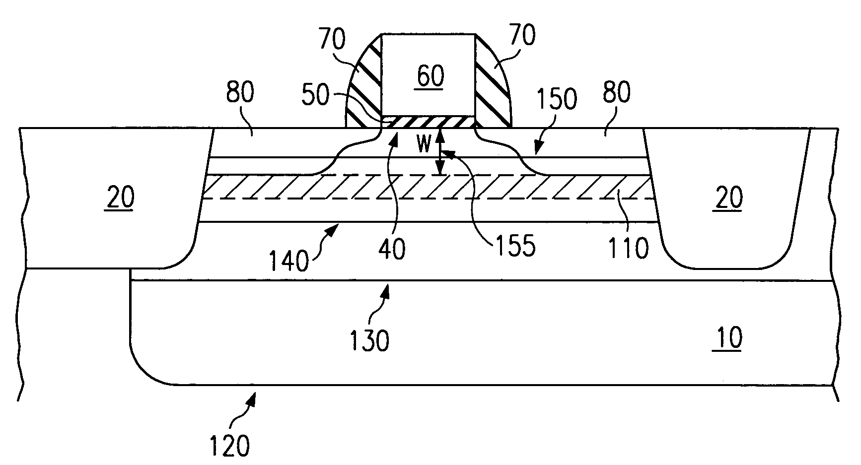
[0005]The improved MOS transistor of this type according to the present invention is characterized by the formation of carbon containing layers. The carbon containing layers will retard diffusion of the dopant species in the various regions of the MOS transistor. The methodology of the present invention offers many advantages over existing technology. The present invention allows for a higher thermal budget in forming the SSRW of advanced CMOS technology which increases dopant activation and hence reduces the “on state” resistance. It is now possible to simultaneously achieve ultra shallow vertical source drain junction conditions and a SSRW. Improved analog matching in individual NMOS and PMOS transistors can now be achieved since the fabrication process is now less sensitive to thermal variations during rapid thermal annealing across the wafer compared to processes that have faster diffusion rates and hence are less well controlled. The technique can be used to balance arsenic diffusion with boron diffusion for fabricating symmetric NMOS and PMOS devices in a typical CMOS process flow. It can also be used to make asymmetric source and drain structures by controlling carbon implantation in the source and drain regions. This may have benefits for making ESD and higher power devices in CMOS circuits. By using a mask to pattern the carbon (or SiGeC) implants it is possible to make a higher threshold and a low threshold voltage device while minimizing source drain implant diffusion in the vertical direction. The methodology allows boron to be extended into scaled deep submicron CMOS technologies, which have had to shift to indium dopants to achieve SSRW and ultra shallow junctions. Although indium works in these technologies it is non-standard for most CMOS processes and has a lower salability limit and is susceptible to carrier freeze out effects at room temperature which limits its usefulness. Other technical advantages will be readily apparent to one skilled in the art from the following FIGUREs, description, and claims.

Problems solved by technology

Although indium works in these technologies it is non-standard for most CMOS processes and has a lower salability limit and is susceptible to carrier freeze out effects at room temperature which limits its usefulness.

Method used


Image

  • Advanced CMOS using super steep retrograde wells
  • Advanced CMOS using super steep retrograde wells
  • Advanced CMOS using super steep retrograde wells

Examples


Embodiment Construction

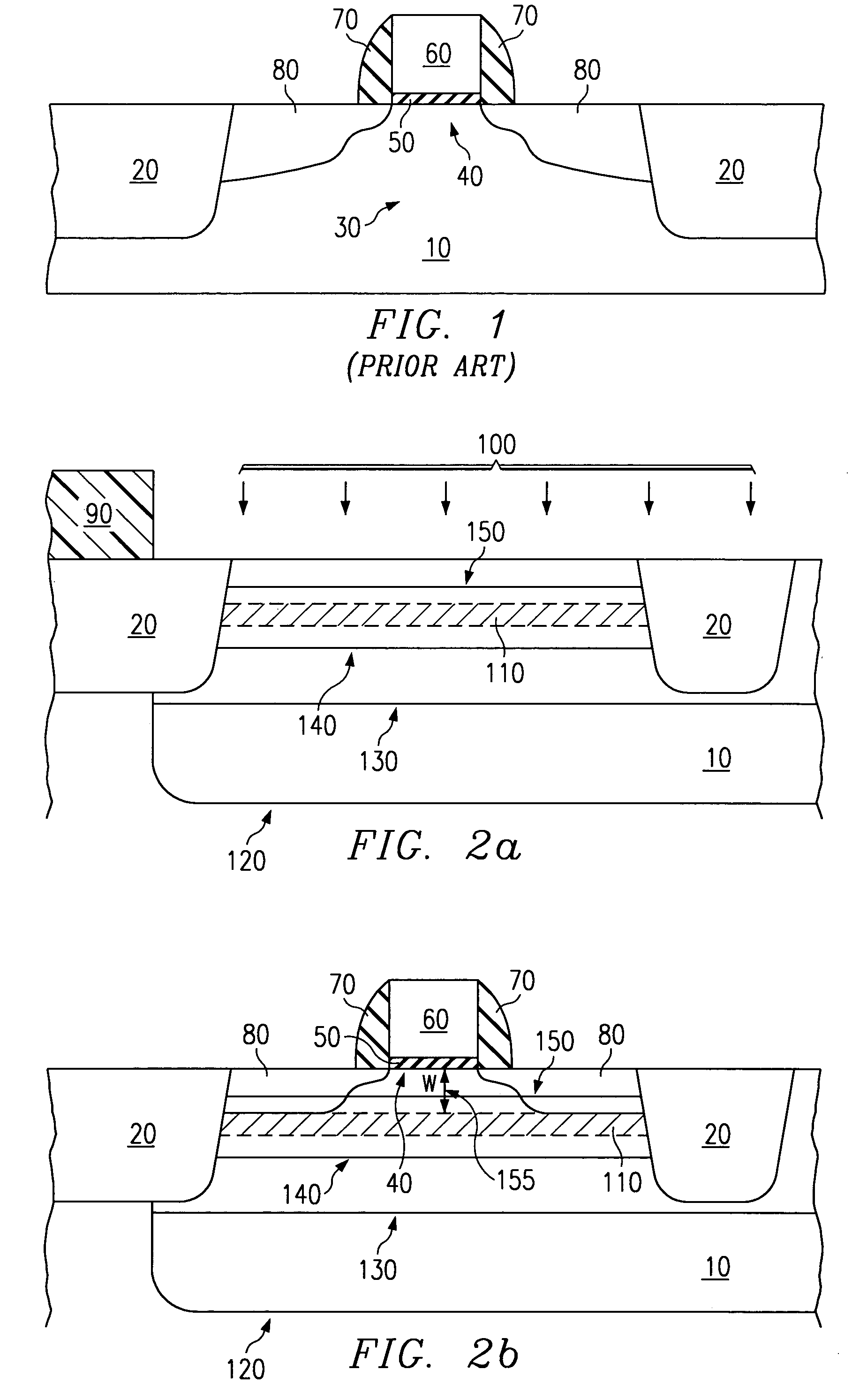
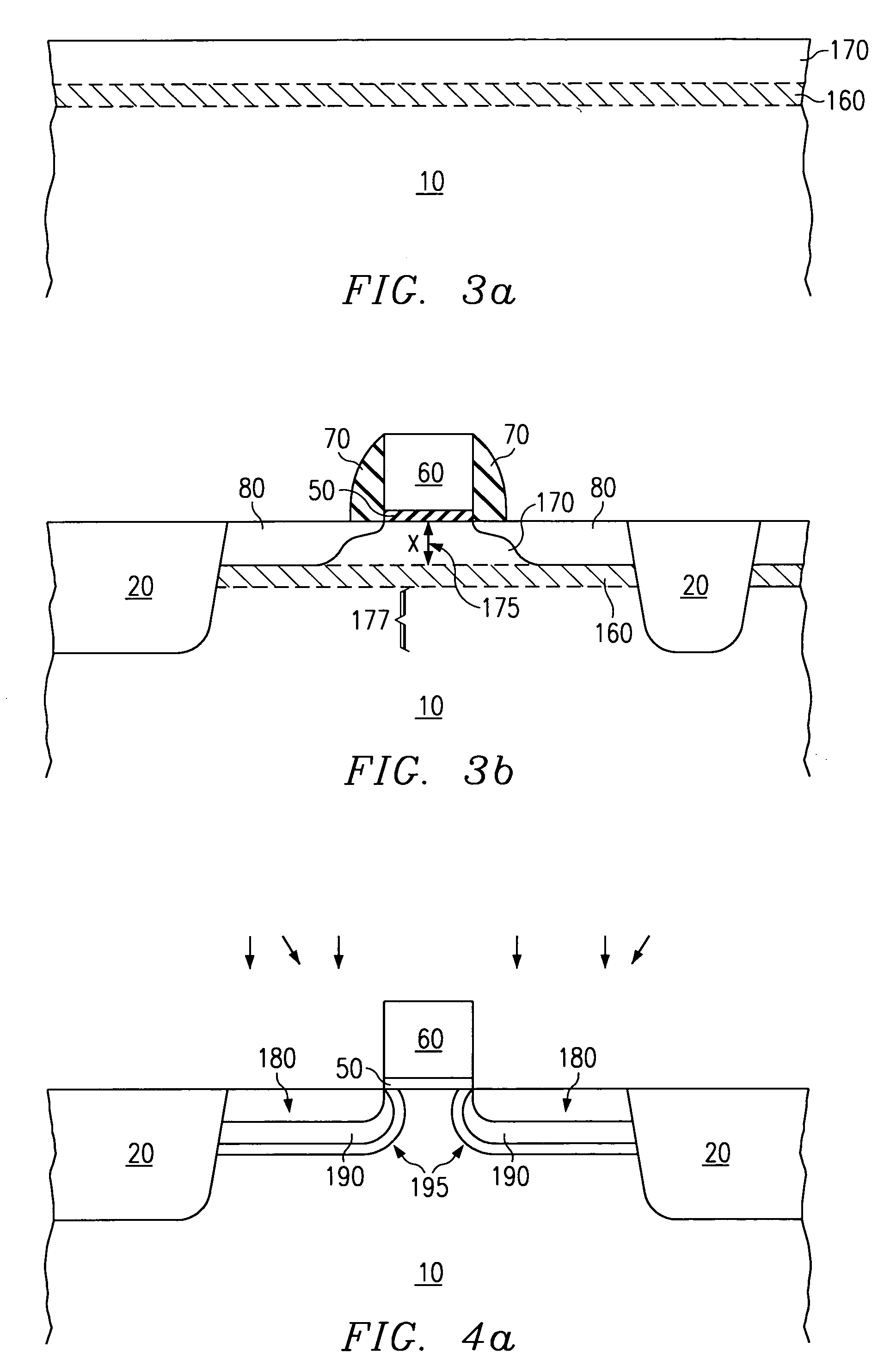
[0014]The invention will be described with reference to FIGS. 2–6. It comprises super steep retrograde well (SSRW) structures formed using a carbon based capping layer. In general the SSRW is very sensitive to diffusion of dopants and the total thermal budget that the SSRW encounters during processing. Transient enhanced diffusion (TED) and the high diffusion rate of boron makes it very difficult to maintain hyper-abrupt SSRW doping profiles during manufacturing. In the instant invention a thin carbon containing film is used as a diffusion barrier-capping layer over the SSRW. This capping layer can be epitaxially grown or implanted. A near intrinsic channel region can then be formed above the capping layer. Ideally this intrinsic channel region is a thin layer that is typically 50 Å to 300 Å in thickness.

[0015]Shown in FIGS. 2(a) and 2(b) are the formation of a SSRW MOSFET using ion implantation. As shown in FIG. 2(a), a silicon substrate 10 is provided and isolation structures 20 a...


PUM


Abstract

The present invention is a method for forming super steep doping profiles in MOS transistor structures. The method comprises forming a carbon containing layer (110) beneath the gate dielectric (50) and source and drain regions (80) of a MOS transistor. The carbon containing layer (110) will prevent the diffusion of dopants into the region (40) directly beneath the gate dielectric layer (50).

Description

[0001]This application claims priority under 35 USC § 119(e)(1) of provisional application Ser. No. 60 / 232,913, filed Sep. 15, 2000.FIELD OF THE INVENTION[0002]The present invention relates to CMOS transistors formed using super steep retrograde wells. The method of formation of the retrograde well involves using a carbon doped capping layer. The method is applicable to both P-Well and N-Well formation by altering the diffusion characteristics of dopants such as B, P, In, and As for optimized retrograde well profile versus total thermal budget seen by these well during subsequent processing steeps.BACKGROUND OF THE INVENTION[0003]As advanced CMOS technology continues to scale and move into the deep-sub-micron geometry dimensions for core devices, proper channel engineering of the CMOS devices becomes increasingly important. One of the more promising methods for extending the performance of CMOS devices as technology continues to scale, is the incorporation of super steep retrograde ...

Claims


Application Information

Patent Timeline
IPC IPC(8): H01L31/119H01L21/265H01L21/336H01L21/8238H01L29/10H01L29/36H01L29/786
CPCH01L21/26506H01L21/823807H01L21/823814H01L21/823878H01L21/823892H01L29/78654H01L29/105H01L29/1083H01L29/66659H01L29/78612H01L29/1045H01L21/26586H01L29/36
Inventor BABCOCK, JEFFREY A.PINTO, ANGELOBALSTER, SCOTTHAEUSLER, ALFREDHOWARD, GREGORY E.
Owner TEXAS INSTR INC
Learn More