Methods and apparatuses for heat treatment of semiconductor films upon thermally susceptible non-conducting substrates

a technology of non-conducting substrates and heat treatment methods, which is applied in the direction of electrical equipment, semiconductor/solid-state device manufacturing, basic electric elements, etc., can solve the problems of high thermal budgets, damage or distortion of glass, damage and/or distortion of used glass substrates, etc., to achieve the goal, improve process uniformity, and increase productivity

US20050186723A1Inactive Publication Date: 2005-08-25VIATRON TECH INC
8 Cites 9 Cited by

Patent Information

Authority / Receiving Office
US · United States
Patent Type
Applications(United States)
Current Assignee / Owner
Publication Date
2005-08-25
Estimated Expiration
Not applicable · inactive patent

Smart Images

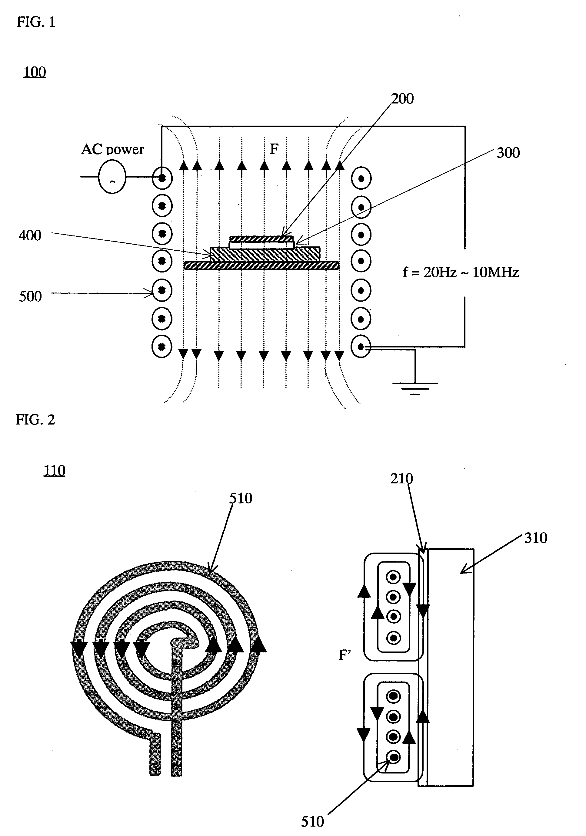
  • Figure 1
    Figure 1
  • Figure 2
    Figure 2
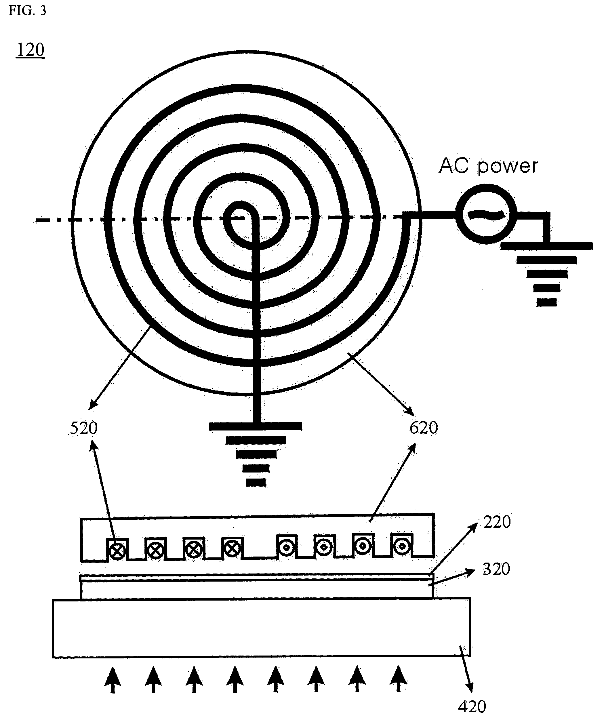
  • Figure 3
    Figure 3
Patent Text Reader

Abstract

In a method for crystallization or dopant activation heat treatment of a semiconductor film upon a thermally susceptible non-conducting substrate lying onto a susceptor, an induction coil is disposed in close proximity of the semiconductor film and disposed with the electrical current direction of the coil aligned parallel to the in-plane direction of the semiconductor film, a magnetic core is disposed around the coil to strengthen and concentrate a magnetic field generated by the coil onto the semiconductor film, and an alternating electrical current is introduced in the induction coil to generate an alternating magnetic field through the semiconductor film heated by the susceptor to the extent that the semiconductor film can be induction-heated.
Need to check novelty before this filing date? Find Prior Art

Description

FIELD OF THE INVENTION

[0001] The present invention relates to methods and apparatuses for heat treatment of semiconductor films upon thermally susceptible non-conducting substrates at a minimum thermal budget. More particularly the invention relates to polycrystalline silicon thin-film transistors (poly-Si TFTs) and PN diodes on glass substrates for various applications of liquid crystal displays (LCDs), organic light emitting diodes (OLEDs), and solar cells. BACKGROUND OF THE INVENTION

[0002] Liquid crystal displays (LCDs) and organic light emitting diodes (OLEDs) grow rapidly in the flat panel displays. In the present time, those display systems employ the active matrix circuit configuration using TFTs. Fabrication of thin film transistors (TFTs) on glass substrate is necessary in those applications.

[0003] TFT-LCDs typically uses the TFTs composing amorphous Si films as an active layer (i.e., a-Si TFT LCD). Recently, interests on the development of TFTs using polycrystalline sil...

Examples

Embodiment Construction

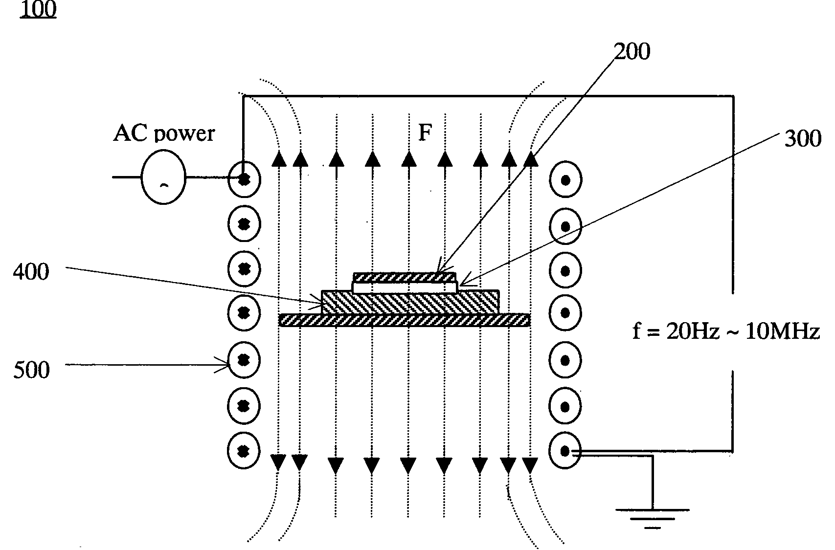
[0056] Referring to FIG. 1, the present embodiment relates to an apparatus allowing low temperature heat treatments of a silicon film on a glass substrate. This apparatus can be used for beat treatments of both crystallization of amorphous silicon and dopant activation of ion-implanted silicon.

[0057] Apparatus 100 consists of a graphite susceptor 400 heating the glass substrate 300 coated with the silicon film 200 and a solenoid induction coil 500 generating magnetic field (F). Introduction of alternating current in the water-cooled induction coil leads to a generation of alternating magnetic field (F). The alternating magnetic flux is utilized for two purposes. First is to heat the graphite susceptor 400 through a function of joule heating effects (i.e., heating mechanism of a conventionally used induction furnace). Second is to enhance the kinetics of heat treatments of silicon films 200 through an inducted emf inside the silicon films 200. In order to see the enhancement effects...