Semiconductor device and method of fabricating the same

a technology of semiconductor devices and semiconductors, applied in semiconductor devices, semiconductor/solid-state device details, electrical apparatus, etc., can solve the problems of large amount of stress applied to bumps, prevent reliable electrical connection, and structural problems in narrow-pitch flip-chip mounting, etc., to achieve high aspect ratio

Inactive Publication Date: 2006-06-20
FUJITSU LTD
View PDF9 Cites 82 Cited by
  • Summary
  • Abstract
  • Description
  • Claims
  • Application Information

AI Technical Summary

Benefits of technology

[0011]The present invention was conceived to overcome the above-described problems, and it is an object of the present invention to provide a semiconductor device with uniform narrow-pitch protruding electrodes with a high aspect ratio.
[0013]This arrangement can achieve a narrow-pitch protruding electrode array, while adequate height of the protruding electrodes is guaranteed. Consequently, the bonding reliability is improved when mounting the semiconductor device on a circuit board in a flip-chip mounting process.
[0021]Since at least one of the ashing process, the acid immersion process, and the water rinsing process is performed before the plating step, the wetting characteristic or the plating-attracting characteristic of the resist mask with respect to plating liquid is improved. Accordingly, the plating liquid is easily introduced into the opening with a high aspect ratio, and protruding electrodes with a sufficient and uniform height can be fabricated.
[0024]This arrangement allows the reducing power to be controlled easily, as compared with the conventional flux reflow process. Because the spread of the solder to the surroundings is well-controlled, short circuits are prevented from occurring between adjacent protruding electrodes.
[0025]Thus, a highly reliable semiconductor device with a narrow-pitch protruding electrode array is realized, while preventing short circuits between adjacent electrodes during the reflow process.

Problems solved by technology

With such a narrow pitch, slight positional offset of the semiconductor chip with respect to the circuit board generally prevents reliable electrical connection.
On the other hand, a structural problem occurs in narrow-pitch flip-chip mounting.
A large amount of stress is applied to the bumps due to difference in the thermal expansion characteristic between the circuit board and the semiconductor chip.
Under large stress on the bumps, the reliability in electrical connection between the semiconductor chip and the circuit board is degraded.
Concerning the fabrication aspect, paste printing is unsuitable for forming narrow pitch solder bumps because the grain size of a typical solder paste is similar to the pitch size.
Ball transfer processes are also unsuitable because such small balls cannot be held reliably.
This makes it difficult for the electrolytic plating liquid to get into the openings of the resist pattern because a resist material generally has a hydrophobic nature and sheds the plating liquid.
If the openings of the resist pattern cannot be sufficiently filled with the electrolytic plating liquid, the thickness of the growing plating layer varies, and uniform-shaped bumps cannot be fabricated.
Such non-uniform bumps greatly reduce the reliability in electrical connection between the semiconductor chip and the circuit board.

Method used


Image

  • Semiconductor device and method of fabricating the same
  • Semiconductor device and method of fabricating the same
  • Semiconductor device and method of fabricating the same

Examples


Embodiment Construction

[0044]The preferred embodiments of the present invention are now described below with reference to the attached drawings.

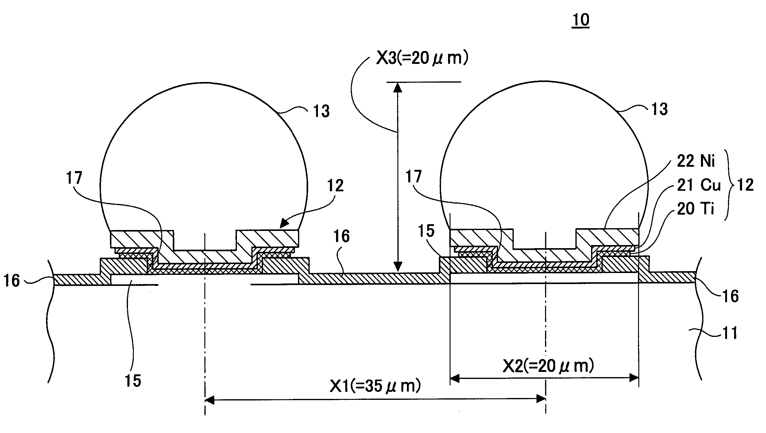
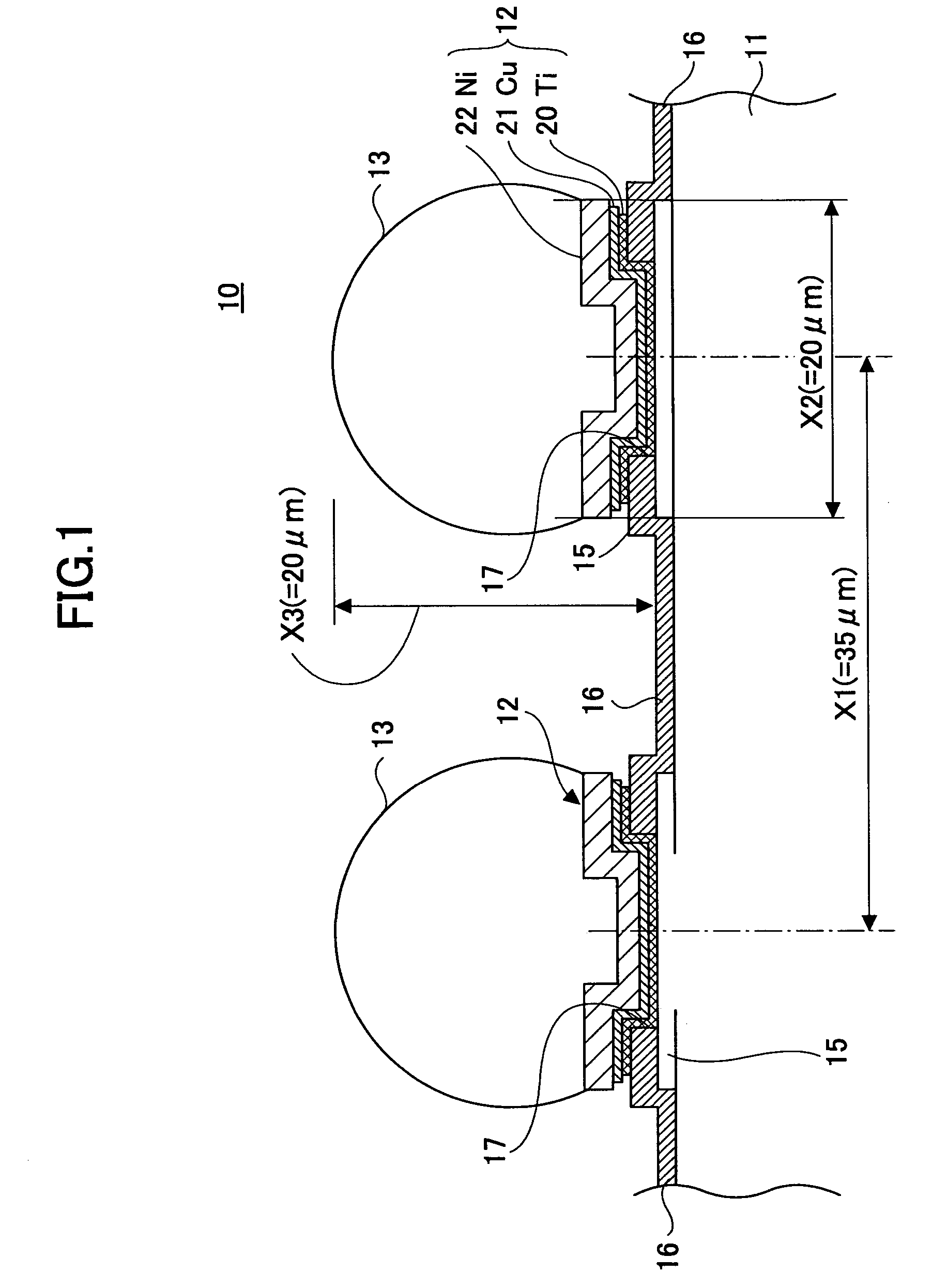
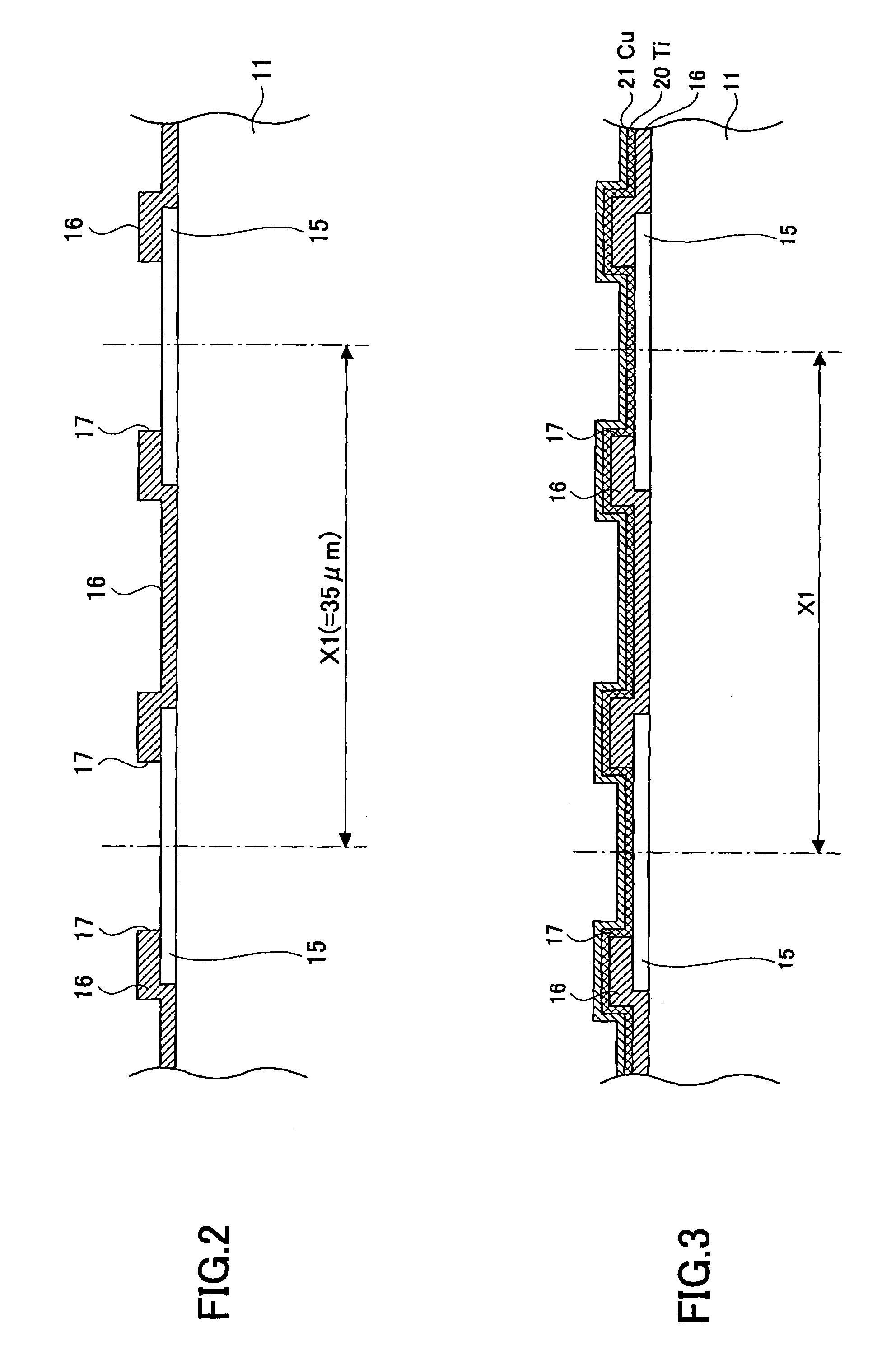
[0045]FIG. 1 is a cross-sectional view of protruding electrodes formed on a semiconductor device via a barrier metal base according to an embodiment of the present invention. Although the preferred embodiment of the present invention is described below using an example of the semiconductor device 10 illustrated in FIG. 1, the present invention is not limited to this example.

[0046]In FIG. 1, a barrier metal base 12 is inserted between a solder ball 13 and an aluminum electrode 15 formed on a semiconductor substrate 11. The semiconductor device 10 is bonded onto a mount board, such as an interposer, by a flip-chip process. The semiconductor device 10 includes the semiconductor substrate 11, the aluminum electrode 15, a cover layer 16 covering a portion of the aluminum electrode 15, the barrier metal base 12 formed on the aluminum electrode 15, and the protruding ele...


PUM


Abstract

A semiconductor device includes a semiconductor substrate and an array of protruding electrodes arranged at a pitch X1. Each of the protruding electrodes has a height X3 and is formed on a barrier metal base of diameter X2 coupled to an electrode arranged on the semiconductor substrate so as to satisfy the relations (X1 / 2)≦X2≦(3*X1 / 4) and (X1 / 2)≦X3≦(3*X1 / 4).

Description

BACKGROUND OF THE INVENTION[0001]1. Field of the Invention[0002]The present invention generally relates to a semiconductor device and its fabricating method, and particularly, to a semiconductor device with narrow-pitch protruding electrodes.[0003]2. Description of the Related Art[0004]In recent years, semiconductor devices incorporated in electric equipment have been made smaller and smaller along with miniaturization of the electric equipment. A semiconductor device or a semiconductor chip has bumps (protruding electrodes) on its device surface, while a circuit board on which the semiconductor chip is placed is furnished with electrodes corresponding to the bumps. The semiconductor chip is mounted on the circuit board through a flip-chip process with the bumps being coupled with the circuit board electrodes. In order to further miniaturize the semiconductor chip, the pitch of the protruding electrodes has to be further narrowed.[0005]Conventionally, protruding electrodes made of s...

Claims


Application Information

Patent Timeline
Patent Type & Authority Patents(United States)
IPC IPC(8): H01L23/48H01L23/52H01L21/60H01L21/28H01L21/768H01L23/02H01L23/485
CPCH01L24/13H01L24/11H01L24/05H01L24/03H01L2224/1147H01L2224/13111H01L2224/13116H01L2924/01013H01L2924/01022H01L2924/01027H01L2924/01029H01L2924/01049H01L2924/01078H01L2924/01082H01L2224/13109H01L2924/014H01L2924/01047H01L2924/01033H01L2924/01023H01L2924/00013H01L2924/01005H01L2924/01006H01L2924/00014H01L2924/0105H01L2224/13099H01L2224/0361H01L2224/03912H01L2224/0401H01L23/52H01L21/60
Inventor ISHIGURI, MASAHIKOMATSUKI, HIROHISAYODA, HIROYUKIOKAMOTO, TADAHIROIKUMO, MASAMITSUCHIBA, SHUICHI
Owner FUJITSU LTD
Why Eureka
Try Eureka