Wear resistant coating with enhanced toughness
a technology of enhanced toughness and wear resistance, applied in the field of cutting tools, can solve the problems of unbalanced dc magnetron sputtering from elemental targets, unbalanced magnetron sputtering from stoichiometric targets, unbalanced magnetron sputtering, etc., and achieve the effect of high toughness
- Summary
- Abstract
- Description
- Claims
- Application Information
AI Technical Summary
Benefits of technology
Problems solved by technology
Method used
Image
Examples
example 1
[0039]Cemented carbide substrates with composition 6 wt % Co and 94 wt % WC were used. The WC grain size was about 1 μm and the hardness was 1650 HV10.
[0040]Before deposition, the substrates were cleaned in ultrasonic baths of an alkali solution and alcohol.
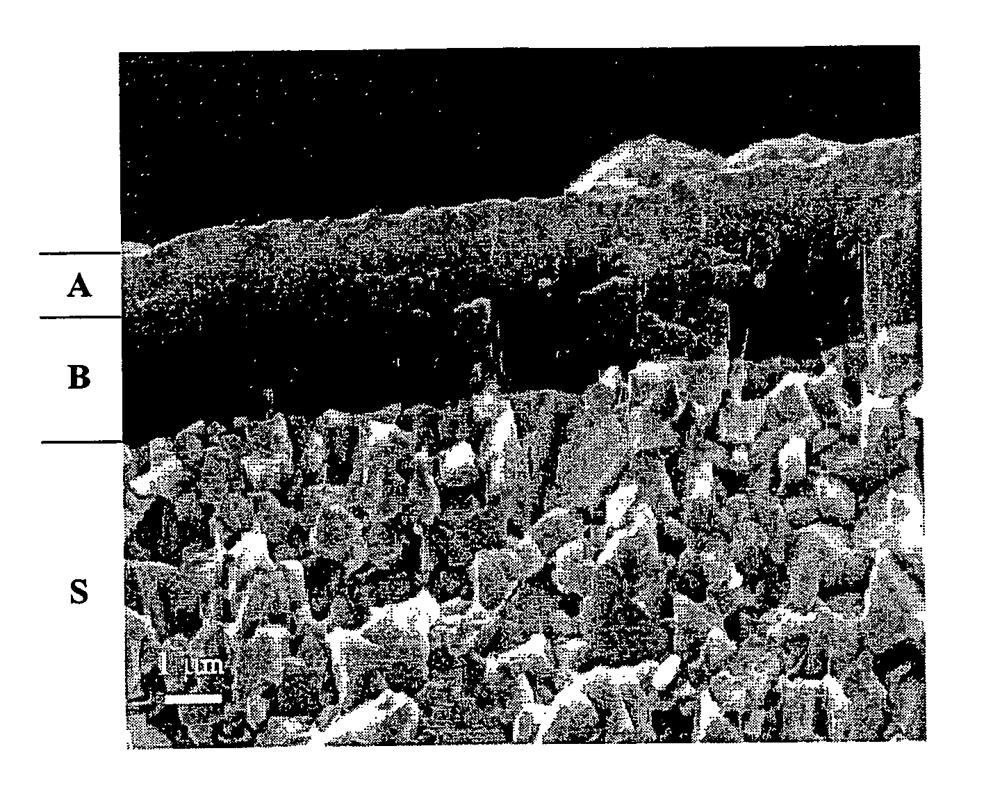
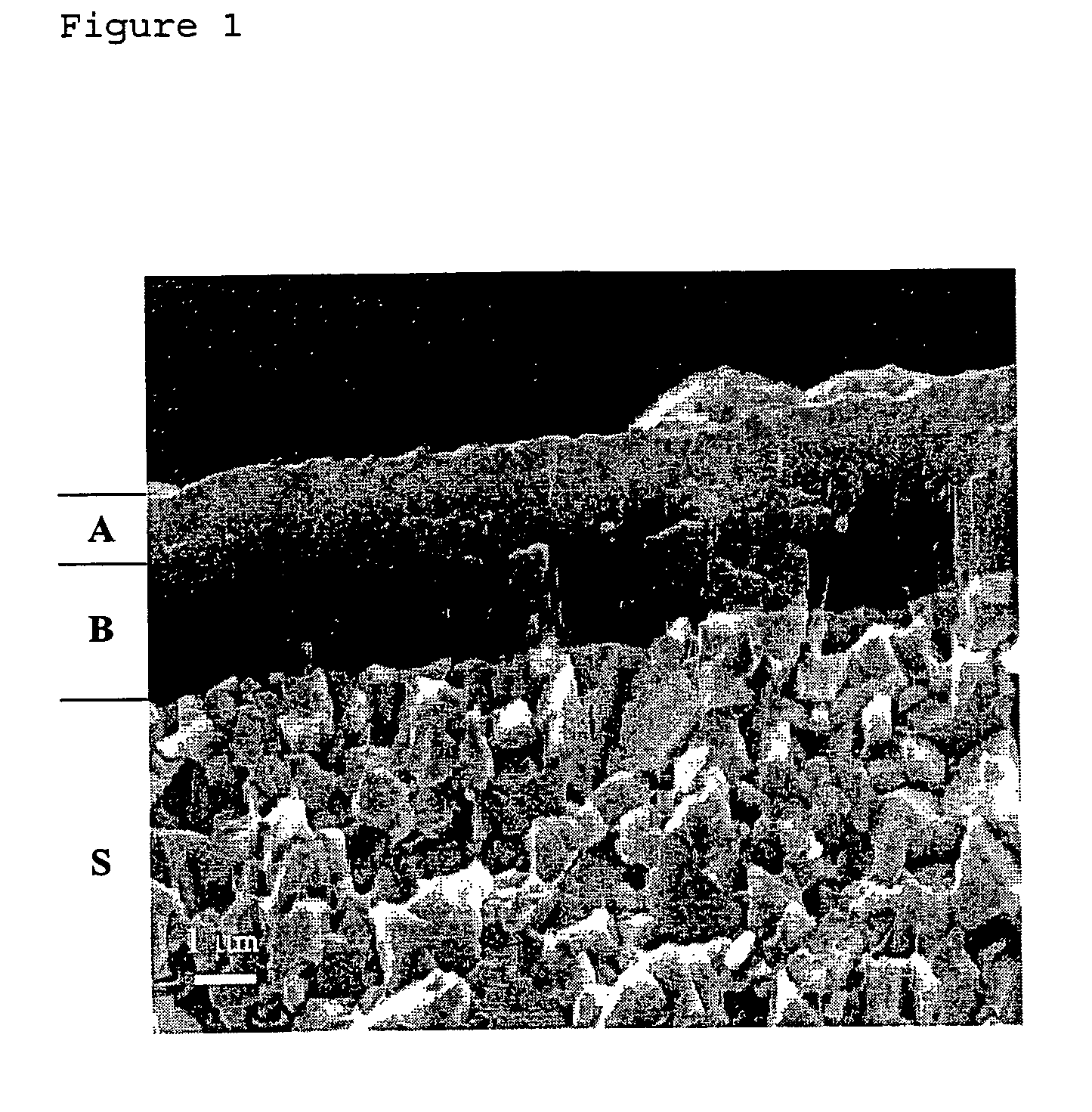
[0041]A first layer of (Ti0.33Al0.67)N was grown using arc evaporation of six Ti / Al (33 at % Ti+67 at % Al) cathodes (63 mm in diameter) in an Ar / N2 atmosphere at total pressure of 2.0 Pa, using a substrate bias of −130 V. The deposition was carried out during 40 min in order to obtain a coating thickness of approximately 2 μm. The deposition temperature was ˜550° C.
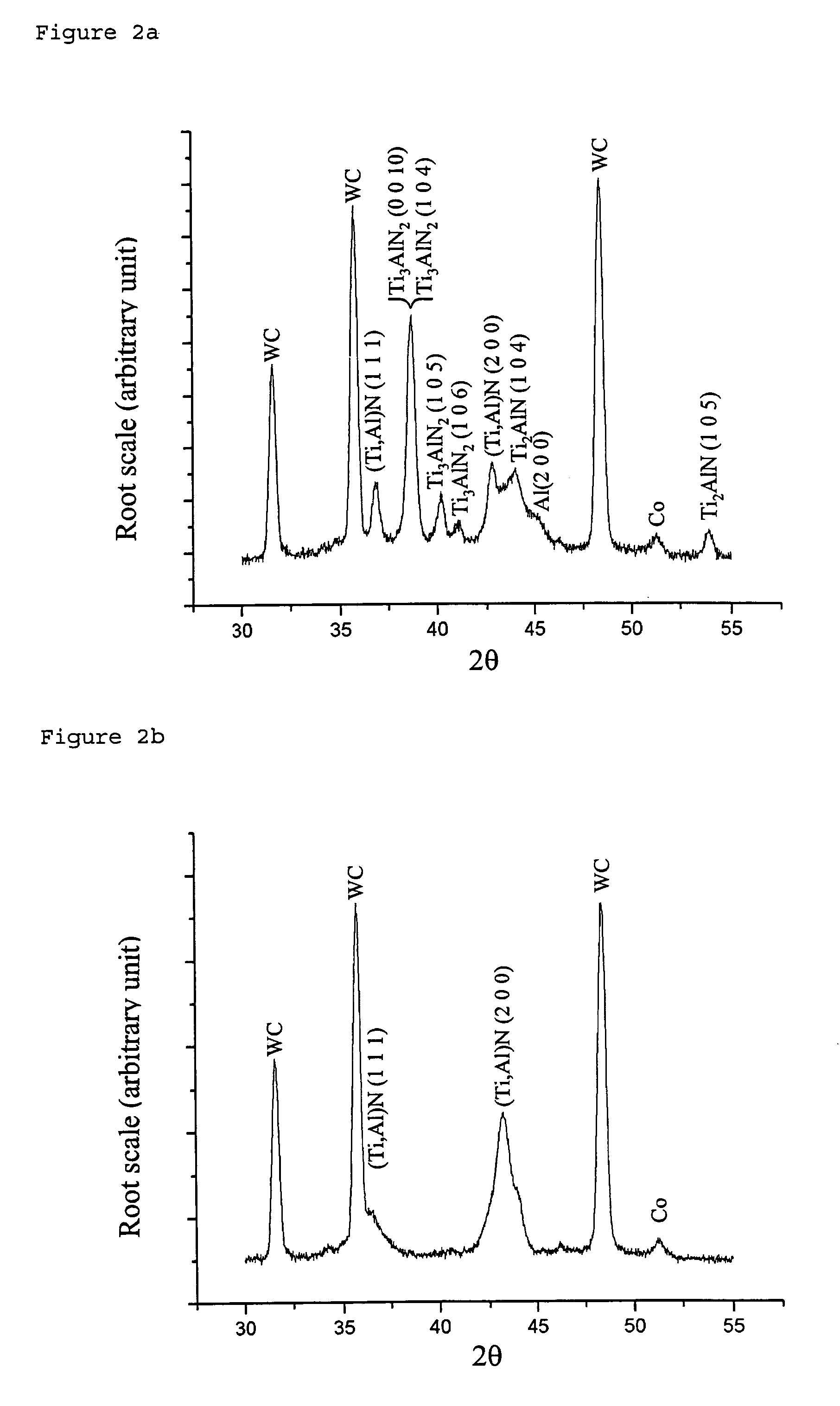
[0042]MAN-layers were deposited on top of the (Ti0.33Al0.67)N layer in a commercially available deposition system aimed for thin film deposition equipped with a dc magnetron sputter source with a 75 at % Ti+25 at % Al target (diameter 63 mm).
[0043]During the magnetron sputtering of the MAN-layer the substrates were stationarily positioned 30 cm from the magnetron and ...
example 2
[0048]Cemented carbide cutting tool inserts, SNGN120408 (WC-6 wt % Co, were coated with a 2 μm thick (Ti0.33Al0.67)N as a first layer and a 1 μm thick MAN-layer according to example 1 variant B. As a reference an insert of similar geometry and substrate, coated with a single layer, similar to the first layer of the MAN coated variant, hereafter called variant D were used.
[0049]A face milling test with interrupted cut was performed in SS2541 (using three 20 mm wide plates separated by 10 mm, mounted as a package), at vc=200 m / min, f=0.1 mm / rev and depth of cut=2.5 mm.
[0050]
VariantTool life, mmFailure modeB2200Chipping and flank wearD1500Chipping
[0051]This test demonstrates the enhanced toughness of the variant with a top MAN-layer compared to a standard coating.
example 3
[0052]The variants according to example 2 were tested in a side milling operation of SS2343. This test is designed to put demands on toughness in combination with low tendency of work material to adhere to the insert.
[0053]The side milling test were performed in SS2343, using a solid work piece, at vc=200 m / min, f=0.1 mm / rev and depth of cut=2.5 mm.
[0054]
VariantTool life, mmFailure modeB2400Chipping and flank wearD1200Chipping
[0055]This test also demonstrates the enhanced toughness in combination with decreased tendency of chip adherence using a top MAN-layer.
PUM
| Property | Measurement | Unit |
|---|---|---|
| Thickness | aaaaa | aaaaa |
| Thickness | aaaaa | aaaaa |
| Length | aaaaa | aaaaa |
Abstract
Description
Claims
Application Information


